
Sentaurus Band Structure
2. Sentaurus Band Structure for 1D confinement
2.1 Input Device Structure
2.2 Initial Solution
2.3 Schrödinger Equation Specification
2.4 Mobility Calculator Specification
2.5 Verifying Material Parameters
2.6 Solution and Saving Output Fields
2.7 Visualizing Outputs
Objectives
- To describe how to set up a structure with 1D confinement for simulating Sentaurus Band Structure using appropriate physics.
2.1 Input Device Structure
To add Sentaurus Band Structure to a Sentaurus Workbench project:
- Choose Tool > Add.
The Add Tool dialog box opens. - Click the Tools button.
- Select the Sentaurus Band Structure icon from the Select DB Tool dialog box.

- Click OK.
Figure 1 shows a Sentaurus Workbench project, where bulk, Silicon-On-Insulator (SOI) and Double Gate (DG) n- and p-MOSFETs are simulated. In those structures, the carriers are confined along one dimension, the vertical direction. The device to simulate with Sentaurus Band Structure is therefore a 1D structure with 1D mesh generated by Sentaurus Process (see Sentaurus Process - Section 2. One-Dimensional Process Simulation), which represents a vertical cross-section of the device in the channel.
Figure 1. Sentaurus Workbench tool flow for Sentaurus Band Structure simulation of n- and p-type devices, and three different types of structure.
The peak of the quantum mechanical carrier density is typically within a couple of nanometers away from the interface between the semiconductor and the insulator, and the wave-function (and therefore the carrier density) decays rapidly from this peak towards the interface. This necessitates having very fine mesh in this interface region, often in the range of 1.5-3 Angstroms.
The input structure file is loaded by:LoadDevice tdrFile=@[relpath n@node|GenerateStructure@_fps.tdr]@This command loads the TDR file from Sentaurus Process with the different materials/regions, the 1D grid, the contacts, and the doping concentration. By default, Sentaurus Band Structure supports Silicon, Oxide and PolySilicon. Material parameters for these materials are loaded at the beginning of the simulation. Default scattering models and default valley models for Silicon are also loaded.
If the input structure contains materials that Sentaurus Band Structure does not support by default, those materials needs to be defined before loading the input structure (see Section 3. Sentaurus Band Structure for 2D Confinement).
2.2 Initial Solution
The top contact is defined by the following statement:
Physics contact=top workfunction=$workfun
where workfun is a Tcl variable for the contact workfunction.
An initial solution of the Poisson equation is recommended with a charge neutral assumption using the classical bulk density models, before solving the Schrödinger equation self-consistently.
In this example, the default crystallographic orientation of the device surface and channel (100)/[100] is considered. An example of how to set the device orientation is shown in Section 3. Sentaurus Band Structure for 2D Confinement.
The Poisson only (using classical DOS) solution is obtained by issuing the following command, and this is done before the Schrödinger equation is defined:
Solve V(top)=$startVg initial logFile=n@node@_epm.plt
The keyword initial here denotes that this solution is to serve as the initial condition for the subsequent Schrödinger solve.
2.3 Schrödinger Equation Specification
Next, the Schrödinger equation is defined through the Math nonlocal construct.
Math nonlocal name=NL1 minZ=0.0 maxZ=@Qbox@For 1D problems, the equation is solved only in a line defined by minZ and maxZ, that represents the vertical direction into the wafer of the channel of a planar bulk MOSFET, an SOI, or DG-FET.
For SOI or DG-FET structures, the variable Qbox is the vertical coordinate of the end of the semiconductor region. For a bulk MOSFET, Qbox must be sufficiently deep into the silicon, where bulk properties and models can be assumed.
To consider wave-function penetration into the dielectric, the nonlocal line must extend into the surrounding dielectric.
After the Schrödinger domain is defined, you need to specify Schrödinger solver (parabolic, k.p, and so on), the valleys that are being simulated (Gamma, L, X valley, and so on), and parameters for the k-space and the energy space.
The Schrödinger solver for the electrons is specified as follows:
Physics nonlocal=NL1 eSchrodinger=Parabolic \
valleys=[list Delta1 Delta2 Delta3] \
Nphi=16 Nk=32 Kmax=0.3 Nsubbands=$Nsubbands \
useDynamicSubbands=1 \
dynamicSubbandEnergyCutoff=$energyCutoff \
a0=5.43e-8 correction=3;
The three valleys (each with degeneracy 2) Delta1, Delta2, and Delta3 are defined by deafult for the silicon conduction band and used here as input of the Parabolic Schrödinger solver.
In general, for the silicon conduction band structure, ConstantEllipsoid, 2kpEllipsoid, or 2kpValley valley models can be used. ConstantEllipsoid is based on the Effective Mass Approximation (EMA). It defines ellipsoidal valleys with effective masses around each band minima. 2kpEllipsoid makes use of ellipsoidal valleys with effective masses that have mechanical strain dependence based on the 2k.p model. The band edges are also modified by the strain. This model balances accuracy and efficiency and it is used to define the default valleys Delta1, Delta2, and Delta3. The full 2k.p (2kpValley) valley model uses a warped, nonparabolic, strain-dependent dispersion, going beyond the simple ellipsoid approximation. The 2k.p model can be used at the cost of increased computation time compared to the previously mentioned models.
For 1D simulation, the k-space is 2D, and exploiting symmetry, the computation is done in a smaller irreducible wedge of the 2D k-space. Sentaurus Band Structure uses polar coordinates. The radial k-grid points are specified by a Kmax and the number Nk in which the Kmax is divided uniformly. Nphi denotes the total number of points spanning 2\pi in the angular dimension.
The dynamic subband feature is activated by the flag useDynamicSubbands=1. In this case, Sentaurus Band Structure automatically determines the number of subbands needed to resolve the carrier density and transport properties. The dynamicSubbandEnergyCutoff parameter controls the energy cutoff above the Fermi level which is considered for the dynamic subband calculation.
Unlike electrons, the hole band structure is more complex. The radial grid is intentionally made non-uniform, because the hole band-structure shows idiosyncratic curvatures near the Gamma point (k=0), and therefore, the radial grid is specified using an explicit list of k-values, where the k-spacings are small close to k=0, and then gradually become larger as k increases. This is specified by the following kGrid list, which is then passed to the Schrödinger equation for holes.
set kGrid [list 0.00E+00 8.35E-03 1.67E-02 2.50E-02 \
                3.33E-02 5.00E-02 6.67E-02 8.33E-02 0.1 \
                0.1167 0.1333 0.15 0.2 0.25 0.3];
For holes, the Schrödinger solver can be specified
as follows:
Physics nonlocal=NL1 hSchrodinger=6kp \
valleys=[list Gamma] \
Nphi=48 kGrid=$kGrid Nsubbands=$Nsubbands \
iwSymmetry=AUTO useKdependentWF=1 \
useDynamicSubbands=1 \
dynamicSubbandEnergyCutoff=$energyCutoff \
a0=5.43e-8;
For the silicon valence band structure, the EMA is insufficient due to its complexity, and typically the 6k.p model is used. The single 6kpValley valley Gamma is defined by default and given here as input to the 6kp Schrödinger solver.
2.4 Mobility Calculator Specification
There are two methods available for calculating the mobility in Sentaurus Band Structure: KGFromK, which evaluates the Kubo-Greenwood integral, and LinearBTE, which uses the linearized Boltzmann Transport Equation to calculate the mobility integral.
The mobility calculator (for electrons) can be specified after the Schrödinger equation is defined in the following way:
Physics nonlocal=NL1 eMobilityCalculator=KGFromK Nphi=32 Nk=128
For holes, the corresponding statement replaces the eMobilityCalculator keyword with the hMobilityCalculator keyword.
2.5 Verifying Material Parameters
Before issuing a Solve statement to compute the solution to the defined system, it is often a good idea to double-check the material parameter definitions. This includes both the mapping of materials to the material/region tags in the input structure, and the definition of the materials known to Sentaurus Band Structure.
This can be checked by the statements:
ListMaterialMap
and
PrintParameters
ListMaterialMap can be used to show how the database materials (which are shown on the left hand side of the command output) are connected to the materials and/or regions in the input structure (shown on the right hand side of the command output).
An example of this output looks like this:List of mappings between material database to device: - Silicon -> Silicon [regions: si1] - Oxide -> Oxide [regions: ox1]
PrintParameters can be used to output the parameters of a specific material, and can also be used for a specific region. It is also possible to save those in output files, as evident in the following commands:
PrintParameters deviceRegion=si1 filename=n@node@_region_si1_mat.txt
PrintParameters dbMaterial=Silicon filename=n@node@_dbmat_Silicon_mat.txt
The output from PrintParameters can also be used to verify the valley and scattering models, and their parameters, that are associated with a material definition.
2.6 Solution and Saving Output Fields
Once the Schrödinger equation is defined, the command:Solve
solves self-consistently the Schrödinger and the Poisson equations.
Following the initial solution (which is done at zero bias), the gate voltage is ramped in a loop, and each subsequent Solve command is passed the increasing gate voltage.
After every Schrödinger solve, the effective electric field is calculated for each gate voltage value by the following statement:
set Eeff [Extract model=eEeffIntegrand region=si1 integral]
The keyword eEeffIntegrand is replaced by the keyword hEeffIntegrand for computing the effective electric field for holes. These models calculate an effective electric field averaged against the carrier density in the inversion layer. The following command is used to push the calculated value into the plt file:
AddToLogFile name=Eeff value=$Eeff
Mobility is calculated for each bias step as a post-processing command of the Schrödinger solution, by using the ComputeMobility statement. The argument xx in the command refers to the component of the mobility tensor along the transport direction x:
set mobXX [ComputeMobility xx]
The solved physical quantities can be saved at each bias step and/or only at the end of the bias ramp, as in this example, by using the Save command in the following way:
Save tdrFile=n@node@_epmZ.tdr models=$saveModels
Here, the saveModels Tcl variable is a list that contains fields like DopingConcentration, ConductionBandEnergy, eDensity, in addition to quantum mechanical solutions that are real-space quantities such as Delta1_0_Wavefunction. Delta1_0_Wavefunction is the wave function of the lowest subband of the Delta1 valley. _0_ denotes the subband index, where the number of the subbands is dynamically determined in this simulation.
It is worth noting that the number of subbands determined within each Solve command can be accessed, and in this example, it is written to screen.
Similar to the real-space quantities, the k-space quantities, like the dispersion relation (E-k plot), scattering rates, IMRT (Inverse Momentum Scattering Rate), can be saved in a separate file using the SaveK command.
2.7 Visualizing Outputs
After the Sentaurus Band Structure tool in this Sentaurus Workbench project there are three Sentaurus Visual tools provided, which show the band structure, the charge density, and the mobility, respectively. Here, a few observations on some of the plots from these Sentaurus Visual nodes is discussed.2.7.1 Band Structure
The PlotBandstructure tool plots three quantities for the subbands of the conduction and valence band valleys as a function of kx and ky: a) the energy dispersion, b) the integrated scattering rate, and c) the inverse momentum relaxation time (IMRT) for all of the scattering mechanisms.
Figure 2 plots the band structure for lowest subband of the three conduction band valleys, Delta0, Delta1, and Delta2, which are the projections on the transport plane of the Silicon bulk band structure ellipsoids, as shown in Figure 3.
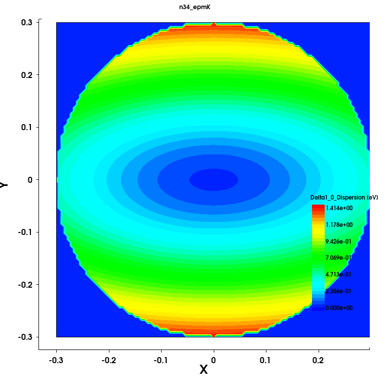
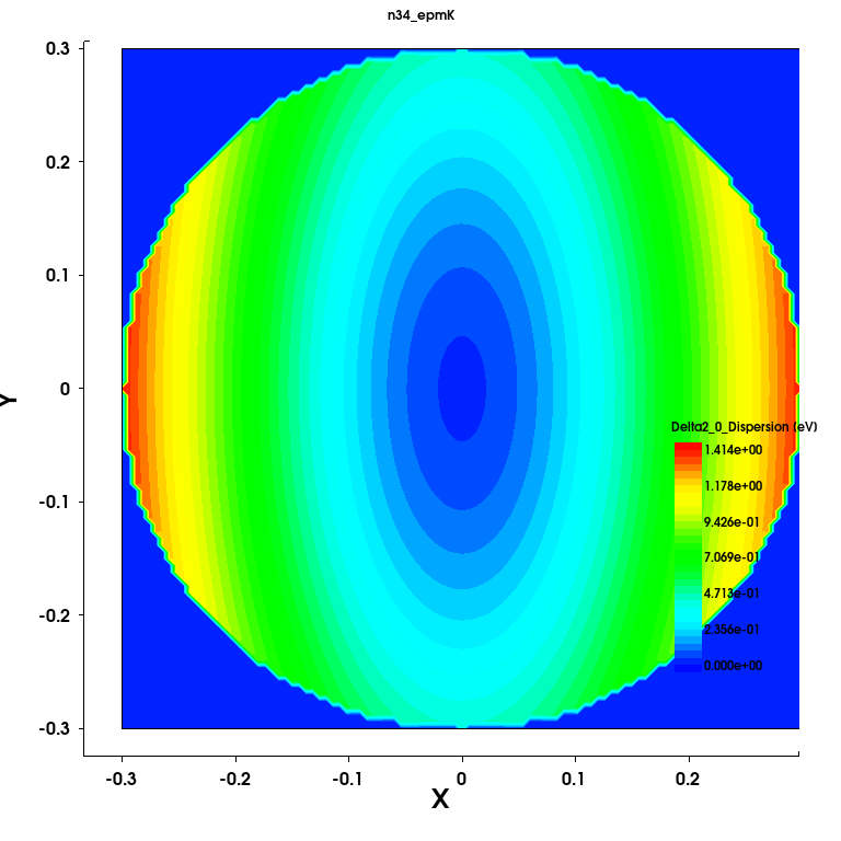
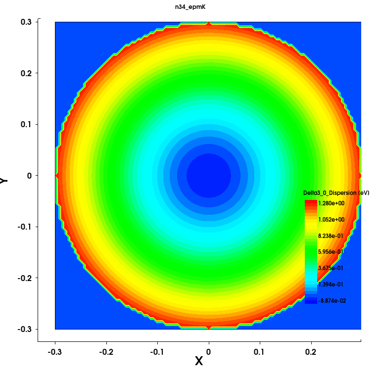
Figure 2. Energy dispersion of Delta valleys of silicon conduction band (in eV) for bulk MOSFET (Device= Bulk) resulting from the Sentaurus Band Structure simulation.
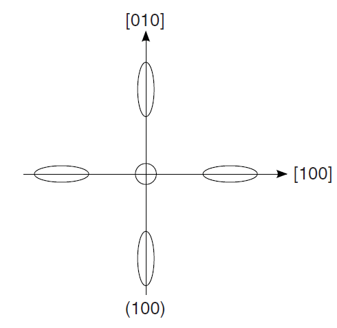
Figure 3. In-plane constant-energy ellipsoids for 1D confinement for Silion (100) surface orientation.
The first three subbands of the Gamma valley are plotted in Figure 4, showing the complex warped shape of the valence band structure.
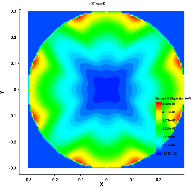
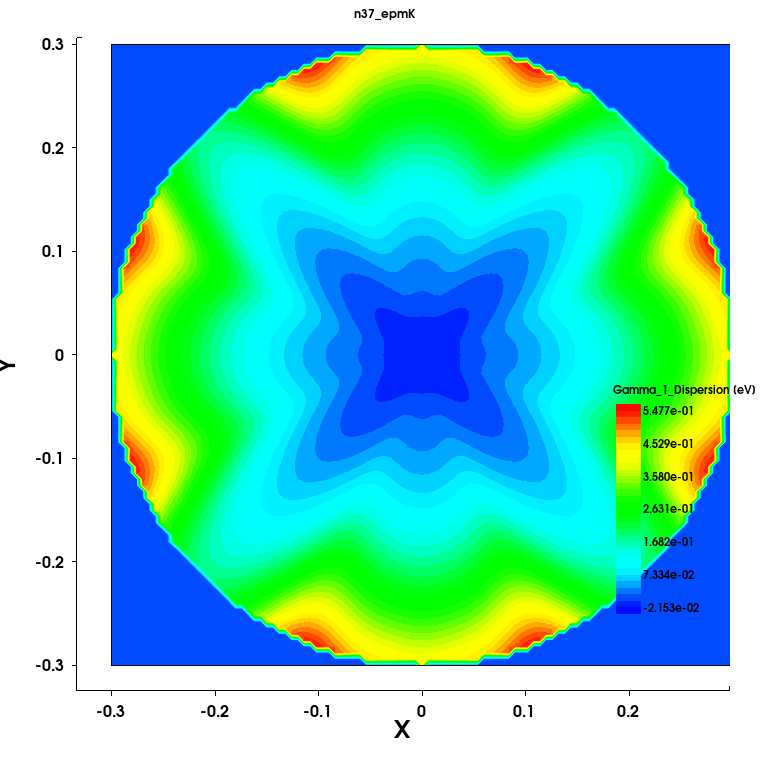
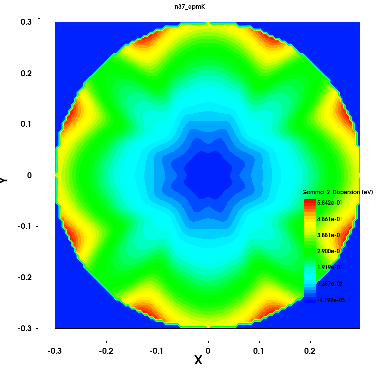
Figure 4. Energy dispersion of the first three subbands of the Gamma valley of silicon valence band (in eV) for bulk MOSFET. (Device=Bulk) from the Sentaurus Band Structure simulation.
The plots for the Scattering Rate and the IMRT from the Delta1 valley are shown in Fig. 5. The IMRT has, in addition to the scattering rate, the local band curvature effect, and can be used to gauge the strength and anisotropy of scattering at a given kx and ky.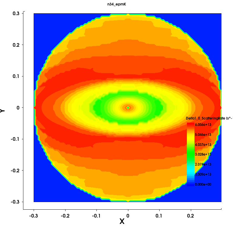
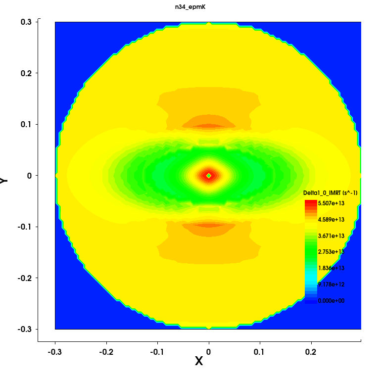
Figure 5. Scattering rate (left) and IMRT (right) for the first subband of the Delta1 valley of Silicon for the MOSFET (Device=Bulk) from the Sentaurus Band Structure simulation.
2.7.2 Density
The quantum mechanical electron density obtained by solving the Schrödinger equations is plotted in Figure 6 for the bulk MOSFET structure, together with the local electron mobility.
In general, Sentaurus Band Structure calculates the effective mobility for the nonlocal line
as the average mobility over all the subbands, weighted by the subband inversion charge.
Hence, the effective mobility has no spatial dependence. However, it is possible to extract a spatial dependent mobility
by weighting each subband mobility value by the subband inversion charge and
the wavefunction norm. For more details, see the Spatial Mobility Profile section of the Sentaurus Device Monte Carlo
User Guide.
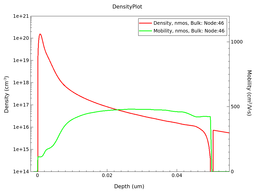
Figure 6. Electron density (left) and mobility (right) in the inversion layer of a MOSFET.
You can also compare the density profile of the bulk, single-gate SOI, and double-gate SOI by plotting all the three corresponding PlotDensity nodes at the same time. This is shown on the left-side axis in Figure 7 for 10-nm Silicon width. (For the MOSFET, this corresponds to the first 10-nm depth). The right-side Y-axis plots the mobility from these three structures. While the double gate structure has a symmetric solution, both the density and the mobility of the single-gate SOI and Bulk MOSFET are similar for the first 5 nm.
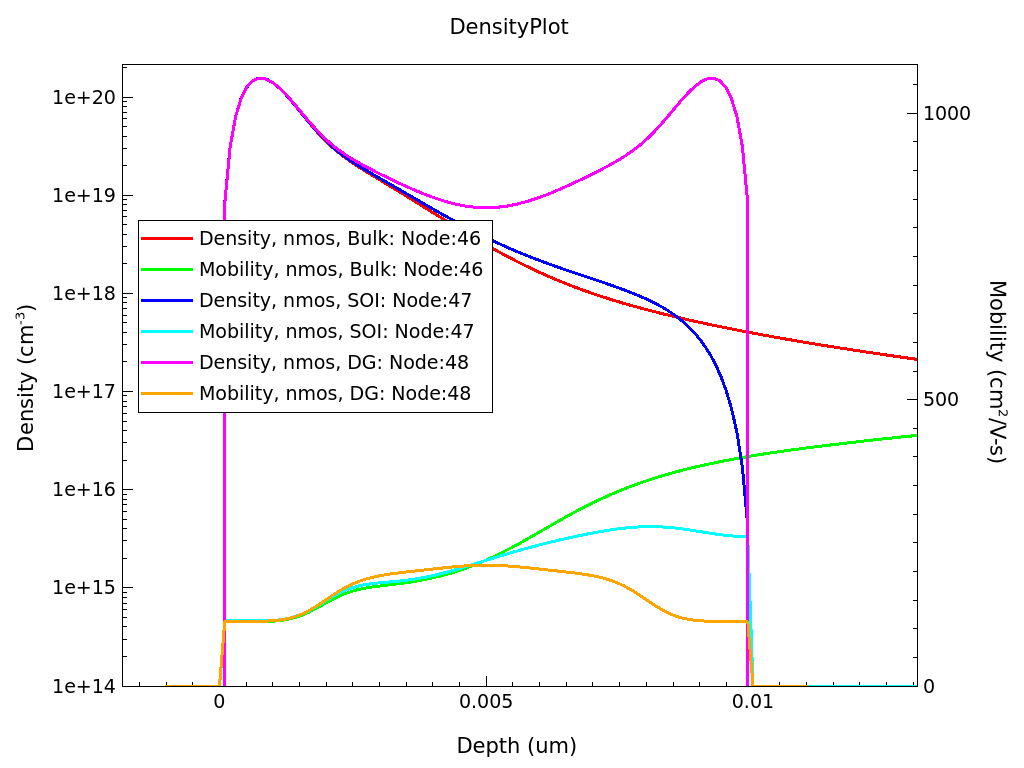
Figure 7. Electron density (left) and electron mobility (right) compared in the three simulated device types - bulk MOSFET, DG, and SOI structures.
2.7.3 Mobility
Finally, the PlotMobility node plots mobility as a function of gate voltage, inversion charge density, and effective electric field. In Figure 8, the electron and hole mobilities for the bulk MOSFET are shown as a function of the effective field. The electron mobility shows significantly larger values compared to the hole mobility.
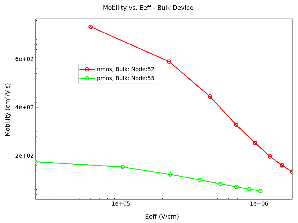
Figure 8. Electron and hole mobilities as a function of effective electric filed for a bulk MOSFET.
Copyright © 2024 Synopsys, Inc. All rights reserved.