 main menu
| module menu
| << previous section
| next section >>
main menu
| module menu
| << previous section
| next section >>
Sentaurus Band Structure
3. Sentaurus Band Structure for 2D confinement
3.1 Workflow and Input Device Structure
3.2 Sentaurus Band Structure 2D - Schrödinger Equation Specification
3.3 Sentaurus Band Structure 2D - Mobility Models and Mobility Calculation
3.4 Sentaurus Band Structure 2D - Solution, Saving Fields and Visualization
Objectives
- To understand how to simulate 2D confinement with Sentaurus Band Structure using appropriate physics.
3.1 Workflow and Input Device Structure
A 2D Sentaurus Band Structure simulation is typically done to evaluate the quantum confinement effect on charge density profile and mobility for a nanowire or nanosheet transistor. You can direclty create a 2D structure that represents a slice in the middle of the channel of the transistor. A simple Gate-All-Around (GAA) structure was first created using the Sentaurus Process tool labeled GAA. Afterward, Sentaurus Mesh is used to slice the GAA structure in the middle of the channel region to create the input structure for Sentaurus Band Structure.
Figure 1 shows the tool workflow for the Sentaurus Band Structure simulation of a 2D cross-section of a GAA transistor. Figure 2 shows the 3D GAA structure from S-Process and the sliced structure from Sentaurus Mesh with its mesh.
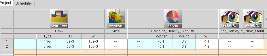
Figure 1. Sentaurus Workbench tool flow for 2D Sentaurus Band Structure simulation. The height (H) and width (W) of the GAA structures, the minimum and maximum gate voltages (VgStart and VgEnd) and the gate work-function (WF) are Sentaurus Workbench parameters. For PMOS, minVg and maxVg are absolute values of the minimum and maximum gate voltage, respectively.
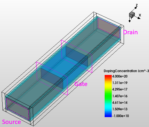
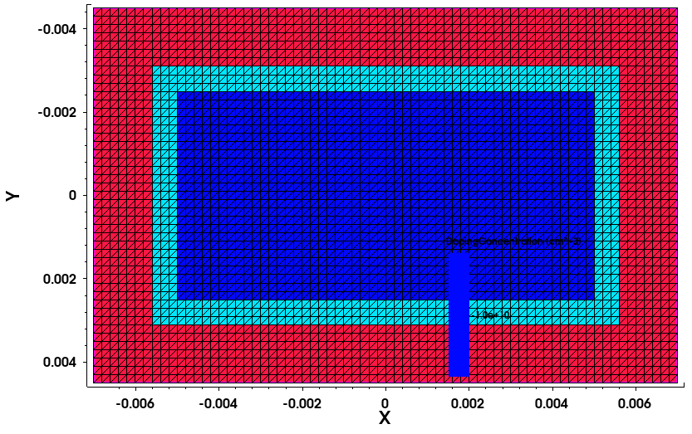
Figure 2. (Left) 3D view of the Gate-All-Around structure with translucent interfacial oxide and silicon regions and (Right) cross-section of the same structure in the middle of the channel region showing the lowly-doped Silicon channel (deep blue), surrounded by Oxide (light blue) and Hafnium DiOxide (red).
3.2 Sentaurus Band Structure 2D - Schrödinger Equation Specification
The basic Sentaurus Band Structure simulation flow remains similar to the 1D case (see Sentaurus Band Structure for 1D confinement). This section covers only the differences and the features that are not explicitly covered in the Sentaurus Band Structure 1D section.
As mentioned in Section 2.1 Input Device Structure, if the input structure has a material that Sentaurus Band Structure does not recognize, it needs to be defined before loading the input structure. This is done by the following statement:
Material name=HfO2 type=InsulatorSuch a material needs to have key parameters defined. In this case, only the Poisson equation is solved in HfO2, and therefore, you need to specify the dielectric constant. If the Schrödinger equation is also solved in the new material, the band structure (valley models and parameters) need to be defined as well. For HfO2, the dielectric constant is defined by:
Physics material=HfO2 Permittivity epsilon=22
To set the crystallographic orientation of the device, you must specify the cristallographic directions of the three axes, as follows:
Physics xDirection=[list 1 1 0] yDirection=[list 0 0 1]
set channelDir [list 1 -1 0]
where channelDir represents the channel direction, and xDirection and yDirection the cross-section coordinates as defined in the loaded TDR file.
After the initial solution, the non-local region where the Schrödinger equation is going to be solved is set up through:Math nonlocal name=NL1 regions=[list Channel]
where Channel is the name of the silicon region.
The 2D Schrödinger solver for the electrons is specified as follows:
Physics nonlocal=NL1 eSchrodinger=Parabolic valleys=$valleylist \
    useDynamicSubbands=1 Nk=32 Kmax=0.6 a0=5.43e-8 correction=3
Unlike the 1D confinement case, where the k-space is 2D (see Section 2.3 Schrödinger Equation Specification), for 2D confinement, the k-space is 1D. Therefore, you need not specify the polar angle discretization parameter Nphi. For the hole band structure, similarl to the 1D simulations, you must specify a non-regular k-grid to have finer mesh near the Gamma point (k=0). The hole Schrödinger solver is then defined as follows:
Physics nonlocal=NL1 hSchrodinger=6kp valleys=$valleylist \
    useDynamicSubbands=1 dynamicSubbandEnergyCutoff=$subbandEnergyCutoff \
    kGrid=$kGrid a0=5.43e-8 useKdependentWF=1 \
    degenSubbandEnergySplit=1.0e-6
Here, the degenSubbandEnergySplit specifies a small value (in eV) that is added to the diagonal of the k�p Hamiltonians to split degenerate subbands.
The Math command is used for setting some numerical controls, as follows:Math potentialUpdateTolerance=3.0e-3 doOnFailure=0In this case, potentialUpdateTolerance specifies in units of the thermal voltage (kT/q) the threshold below which the potential update is considered converged. doOnFailure is a flag which allows the simulation to proceed to the next bias point and seek a solution even if the calculation does not converge at a previous bias condition. The initial Poisson only condition is resolved once the Schrödinger equation is defined on the slice before ramping the gate bias.
3.3 Sentaurus Band Structure 2D - Mobility Models and Mobility Calculation
The surface roughness (SR) and Coulomb scattering models are explicitly defined in this example. For SR scattering for electrons, the following statement sets up the generalized Prange-Nee model for the semiconductor-insulator boundaries (see the Sentaurus Device Monte Carlo User Guide for details) for intravalley transitions between the valleys specified in the valleylist:
Physics material=all ScatteringModel=SRFor2D name=ElectronSR \
    transitionType=Intravalley valleys=$valleylist \
    delta=[list {100 0.3e-7} {110 0.3e-7}] lambda=1.5e-7 powerSpectrum=Exponential beta=1.5
An exponential power spectrum is selected with exponent of 1.5 (beta=1.5) for the silicon-insulator interface. The parameter lambda sets the correlation length of the silicon-insulator roughness to 1.5 nm. The amplitude of the roughness delta is specified as a list of two pairs, where the first value is the surface orientation and the second value the corresponding amplitude. In this case, a value of 0.3 nm is set for both (100) and (110) orientations. The hole SR scattering model is defined in a similar manner:
Physics material=all ScatteringModel=SRFor2D name=HoleSR \
    transitionType=Intravalley valleys=$valleylist \
    delta=[list {100 0.25e-7} {110 0.25e-7}] lambda=4.0e-7 powerSpectrum=Exponential beta=1.5
The impurity scattering model, or Coulomb scattering model, is defined for electrons as follows:
Physics material=all ScatteringModel=Coulomb name="eCoulomb" scaleFactor=1.0 \
    transitionType=Intravalley valleys=$valleylist screening=Lindhard \
    whenToCompute=FirstIteration
scaleFactor is an adjustable parameter, which can be used to increase or
decrease the strength of the Coulomb scattering rate. The Coulomb scattering depends on the doping concentration in the structure
that is automatically read by the Coulomb scattering model.
3.4 Sentaurus Band Structure 2D - Solution, Saving Fields and Visualization
The gate bias is ramped from the VgStart value to VgEnd value in 0.1-V steps. Sentaurus Band Structure self-consistently solves the Poisson equation and the Schrödinger equation at each gate voltage:
for {set Vg @VgStart@} {$Vg<=[expr @VgEnd@+0.001]} {set Vg [expr $Vg + 0.1]} {
    # Vg for filename
    set Vg_print [format %.2f $Vg]

    Solve V(gate)=[expr $carsign*$Vg]  logFile=n@node@_epm.plt
The volumetric inversion layer density Ninv is extracted and added to the log file. The mobility is calculated using the ComputeMobility command and added to the log file.
set Ninv_cm [getNinv]
puts "Ninv as is = [format "%.3e" $Ninv_cm] cm-1"
# Compute inversion density per cm2
set Ninv_cm3 [expr $Ninv_cm/(@W@*1e-4)/(@H@*1e-4)]
puts "Ninv/vol = [format "%.3e" $Ninv_cm3] cm-3"
AddToLogFile name=Ninv value=$Ninv_cm3
AddToLogFile name=MobilityXX value=[ComputeMobility xx]
Because the number of subbands to be used is a dynamic quantity, for each solution the actual number of subbands used can be obtained by the [Physics getSubbandNumbers] command and then the real space quantities such as wave functions and densities can be saved for each subband.
The [ComputeMass] command is used to calculate the mass along the different directions for some of the subbands of the different valleylist simulated.
The Sentaurus Visual tool Plot_Density loads the 2D nanosheet cross-section from the previous Sentaurus Band Structure node for two different gate biases, above the threshold voltage at 0.6 V and in strong inversion at 0.9 V. Cutlines are taken at the center of the nanosheet, and the carrier density profiles are shown in the bottom half of the plot. These plots are reported in Figure 3 for nanosheet structures having a 5 nm x 10 nm cross-section.
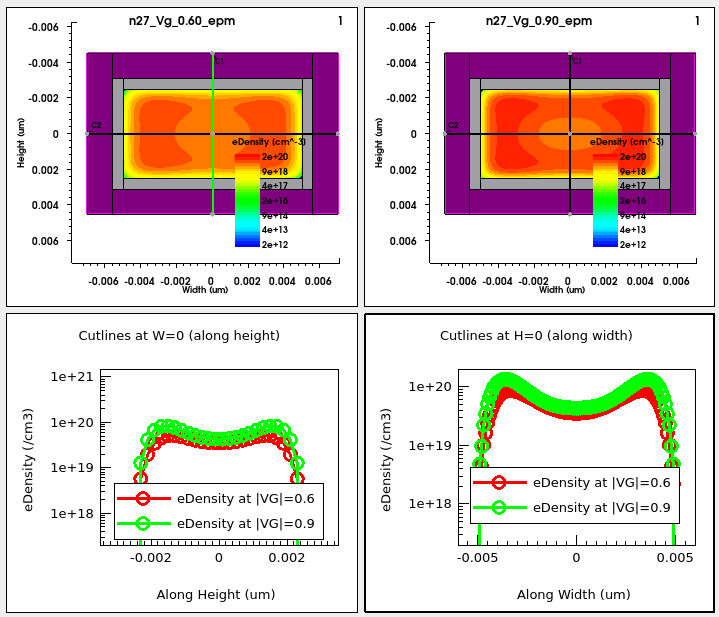
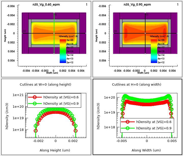
Figure 3. (Top) 2D electron density profiles for two different gate biases (0.6 V and 0.9 V) and cutlines of the same in the middle of the channel along the width (X=0) and along the height (Y=0). (Bottom) Corresponding hole density profiles at gate biases -0.6 V and -0.9 V.
The Plot_Ninv_Mobility tool plots the mobility on the Y1 axis and the normalized volumetric carrier density on the Y2 axis for three different nanosheet cross-sections, having height of 5 nm, and widths of 5 nm, 10 nm, and 15 nm, respectively. The plots are shown in Figure 4 for electrons and holes.
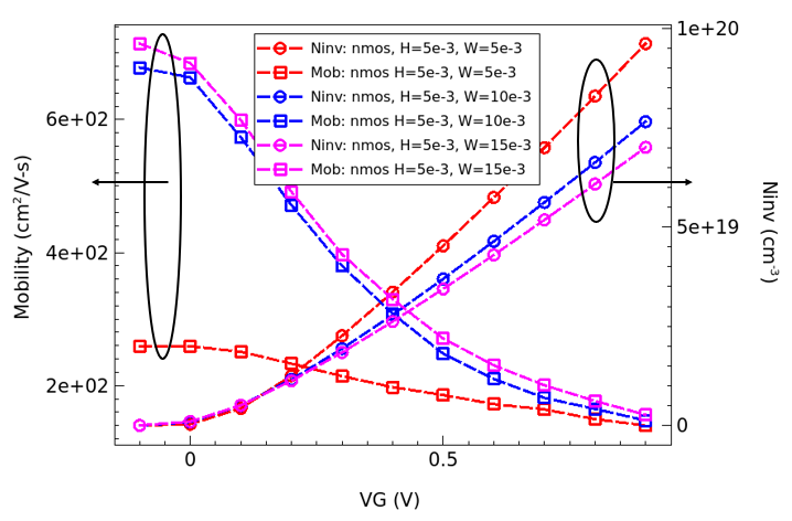
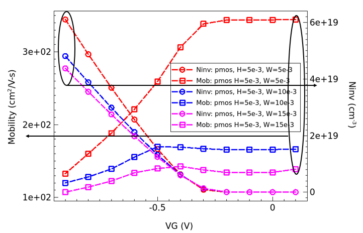
Figure 4. Mobility on the Y1 axis and the normalized volumetric carrier density on the Y2 axis for three different widths of a 5-nm thick nanosheet for electrons (Top) and holes (Bottom)
main menu | module menu | << previous section | next section >>
Copyright © 2024 Synopsys, Inc. All rights reserved.