 main menu
| module menu
| << previous section
| next section >>
main menu
| module menu
| << previous section
| next section >>
Sentaurus Device
19. Special Focus: Tunneling
19.1 Overview
19.2 Example: MOS Gate Tunneling Current
19.3 Example: Schottky Diode
19.4 Example: SONOS Memory
19.5 Example: Tunnel Diode
19.6 Assignment
Objectives
- To demonstrate the use of tunneling models available in Sentaurus Device.
19.1 Overview
Tunneling is a very important physical effect in current microelectronic devices. This section presents various tunneling models available in Sentaurus Device with examples:
- Fowler–Nordheim model – the simplest
- Direct tunneling model – the next most powerful
- Nonlocal tunneling model – the most versatile
- Dynamic nonlocal path band-to-band tunneling model
19.2 Example: MOS Gate Tunneling Current
In this section, you will apply various tunneling models to estimate the gate tunneling current in a MOS capacitor.
The complete project can be investigated from within Sentaurus Workbench in the directory Applications_Library/GettingStarted/sdevice/Tunneling/MOS_Gate_Tunneling.
The simulations are organized in the Sentaurus Workbench project as shown in Figure 1. The tool flow starts with Sentaurus Structure Editor, which generates the MOS capacitor. The Sentaurus Device tool instance Tunneling simulates the gate tunneling current of the MOS capacitor. The Sentaurus Visual tool instances next to the Sentaurus Device tool instances plot the respective I–V characteristics.
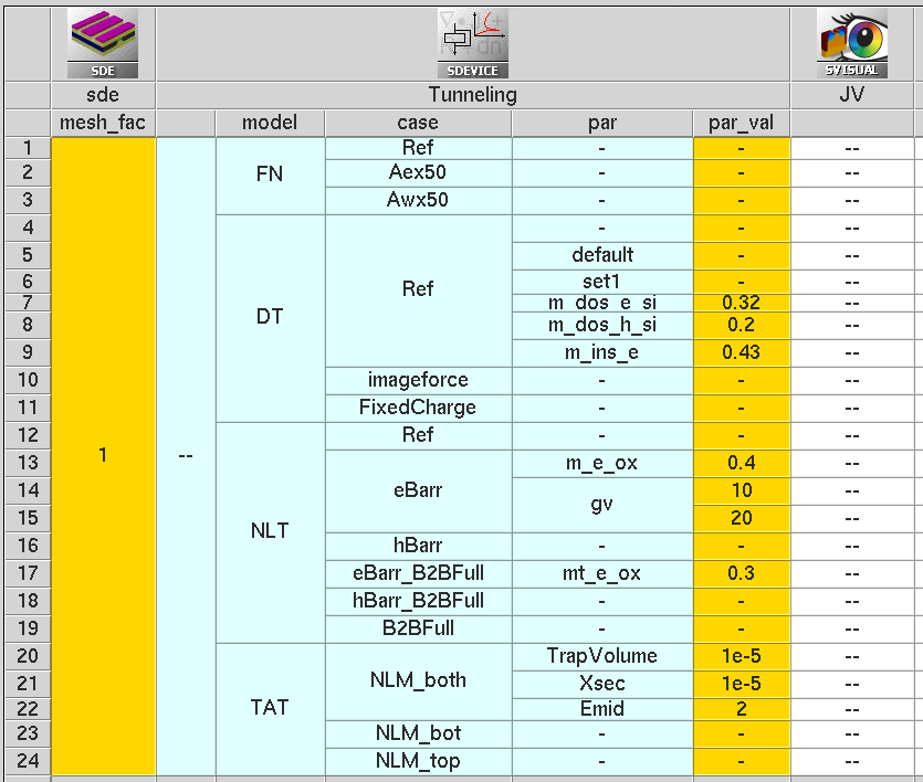
Figure 1. Organization of project in Sentaurus Workbench. (Click image for full-size view.)
The Sentaurus Workbench parameter model denotes the tunneling model invoked, and the parameter case is the label for the different simulation cases. The case Ref uses the default parameter set for the model invoked. Figure 2 shows the MOS structure used in this example.
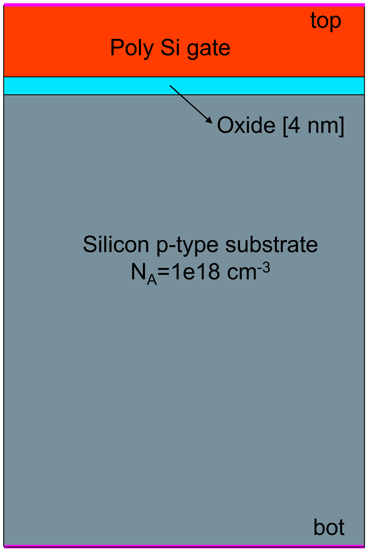
Figure 2. MOS structure used in this example. (Click image for full-size view.)
This section presents the following topics:
- Section 19.2.1 Fowler–Nordheim Model
- Section 19.2.2 Direct Tunneling Model
- Section 19.2.3 Nonlocal Mesh
- Section 19.2.4 Nonlocal Tunneling Model
- Section 19.2.5 Nonlocal Tunneling for Traps (Trap-Assisted Tunneling)
19.2.1 Fowler–Nordheim Model
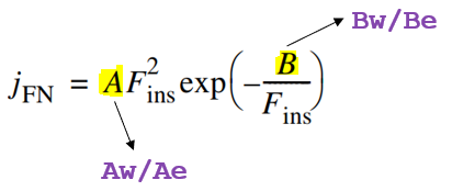
The Fowler–Nordheim tunneling model is simpler and a numerically efficient tunneling model among the other models. The tunneling current density is given by the following expression. It also notes the model parameters that can be modified in the parameter file.
Usage: The model is activated by specifying the option Fowler to the GateCurrent in the appropriate interface Physics section of the command file:
Physics(RegionInterface="r.box/r.channel") {
   GateCurrent(Fowler GateName="top")
}
The specification of model parameters is optional. The default parameter set is used if a parameter set is not modified. The parameters can be modified in the FowlerModel parameter set. The default parameter set as shown here is used for the Ref case:
RegionInterface="r.box/r.channel" {
   FowlerModel
   {
	Aw	= 1.23e-06	# [A/V^2]
	Bw	= 2.37e+08	# [V/cm]
	Ae	= 1.87e-07	# [A/V^2]
	Be	= 1.88e+08	# [V/cm]
	Gm	= 1		# [1]
   }
}
The Fowler–Nordheim tunneling current is implemented as a current boundary condition at the interface where the current is produced and, as such, Fowler–Nordheim parameters must be defined for an interface and not for a region (insulator or semiconductor).
Sentaurus Device uses different parameters (denoted by e for erase and w for write) depending on the direction of the electric field between the contact and semiconductor in the oxide layer. Erase is applicable when the electric field points from the semiconductor to the metal (semiconductor at a relatively higher potential than metal). Conversely, write parameters are applied when the electric field points from metal to semiconductor. For Aex50, the parameter Ae is increased by 50× with all other parameters remaining the same as that of Ref. Similar notation is used for Awx50.
Figure 3 plots the J–V characteristics for these three cases. As can be seen, for Aex50, the current density changes only for positive electric fields. For negative electric fields, the current density is the same as that of Ref. Similar behavior can be seen for Awx50.
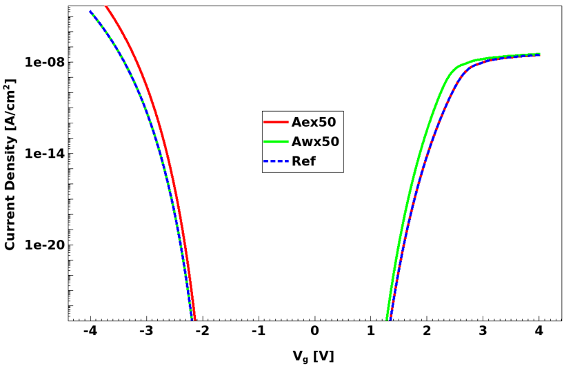
Figure 3. Fowler–Nordheim tunneling current. For Ref, the default parameter set is used. For Aex50, the parameter Ae is increased by 50× with all other parameters remaining the same as that of Ref. Similar notation is used for Awx50. (Click image for full-size view.)
The output file (*_des.out) further notes the differences compared with the default parameters. For example, the output file for Awx50 prints the following (note the change in the Aw parameter):
...
---------------------------------------------------
 Reading parameters for region interface "r.box/r.channel"
---------------------------------------------------

   Differences compared with default parameters:
   Value of A for writing: Aw = 6.1500e-05, instead of: 1.2300e-06 [A/V^2]
...
The Fowler–Nordheim model assumes a triangular barrier at the metal or semiconductor to dielectric interface. Figure 4 shows the band diagrams for the MOS structure for two gate bias conditions (Vg= 0 V and Vg= 4 V). For the high electric field case (Vg= 4 V), the barrier is triangular in shape but, for the low electric field case (Vg= 0 V), the barrier becomes trapezoidal. Owing to this deviation from a triangular barrier assumption, for low fields and for thin (< 3 nm) oxides, the Fowler–Nordheim model underestimates the tunneling current (see Figure 5).
The direct tunneling model is the next most powerful model that overcomes this limitation. The direct tunneling model works for both trapezoidal (low field) and triangular (high field) barrier conditions and, therefore, supersedes the Fowler–Nordheim model.
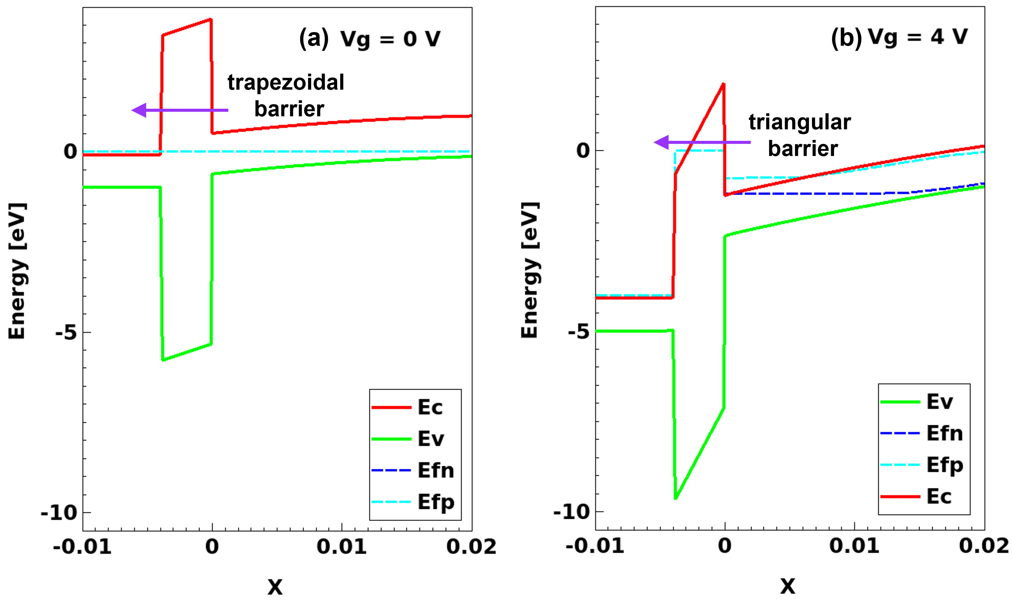
Figure 4. MOS band diagrams. (Click image for full-size view.)
For most purposes, you should use the direct tunneling model rather than the Fowler–Nordheim model as the former is much more versatile.
19.2.2 Direct Tunneling Model
Direct tunneling is the dominant gate leakage mechanism for oxides thinner than 3 nm. The direct tunneling model assumes a trapezoidal barrier and covers both direct tunneling and the Fowler–Nordheim regimes. Direct tunneling turns into Fowler–Nordheim tunneling at oxide fields higher than approximately 6 MV/cm, independent of the oxide thickness.
Model and Related Parameters: The following expressions summarize the model for electrons, noting the parameters that can be modified in the parameter file.
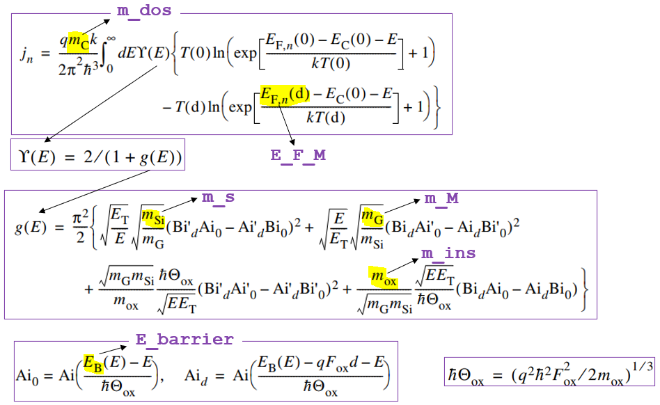
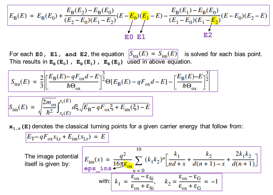
Barrier lowering (optional) due to image forces (image force effect) is included in the model by taking \(E_{\text"B"}(E)\) as an energy-dependent pseudobarrier. If the image force effect is neglected, then \(E_{\text"B"}(E)\) is the bare barrier height \(E_{\text"B"}\), which is an input parameter.
Usage: The model is activated by specifying the keyword DirectTunneling in the Physics section of the command file as shown:
Physics(RegionInterface="r.box/r.channel") {
   GateCurrent(DirectTunneling GateName="top")
}
The specification of model parameters is optional. The default parameter set is used if the parameter set is not modified. The parameters can be modified in the DirectTunneling parameter set. The default parameter set as shown here is used for the Ref case:
RegionInterface="r.ox/r.si" {
   DirectTunneling
   {
	eps_ins	= 2.13         	 # [1]
	E_F_M	= 11.7           # [eV]
	m_M	= 1              # [m0]
	m_ins	= 0.5 ,	0.77	 # [m0]
	E0	= 0 ,	0	 # [eV]
	E1	= 0 ,	0	 # [eV]
	E2	= 0 ,	0	 # [eV]
	m_s	= 0.19 , 0.16	 # [m0]
	m_dos	= 0.32 , 0.3	 # [m0]
	E_barrier = 3.15 , 4.73	 # [eV]
   }
}
If tunneling occurs between two semiconductors (semiconductor-insulator-semiconductor), then the coefficients for metal (m_M and E_F_M) are not used. In addition, the parameters eps_ins, m_ins, m_dos, E0, E1, and E2 must be same for the two semicondutor-insulator interfaces. Sentaurus Device reports the “Inconsistent parameters for Schenk's direct tunnelling model. !” error message if these parameters are not the same for the two interfaces. The E_barrier and m_s parameters can be different for the two interfaces.
Figure 5 (left) shows the comparison of the direct tunneling current to Fowler–Nordheim tunneling. For DT Ref, the default parameter set is used. As can be seen, the Fowler–Nordheim model underestimates the tunneling current for lower gate-bias electric fields. For DT imageforce, the image force barrier lowering option is switched on by modifying the E1 and E2 values to 0.3 and 0.7, respectively.
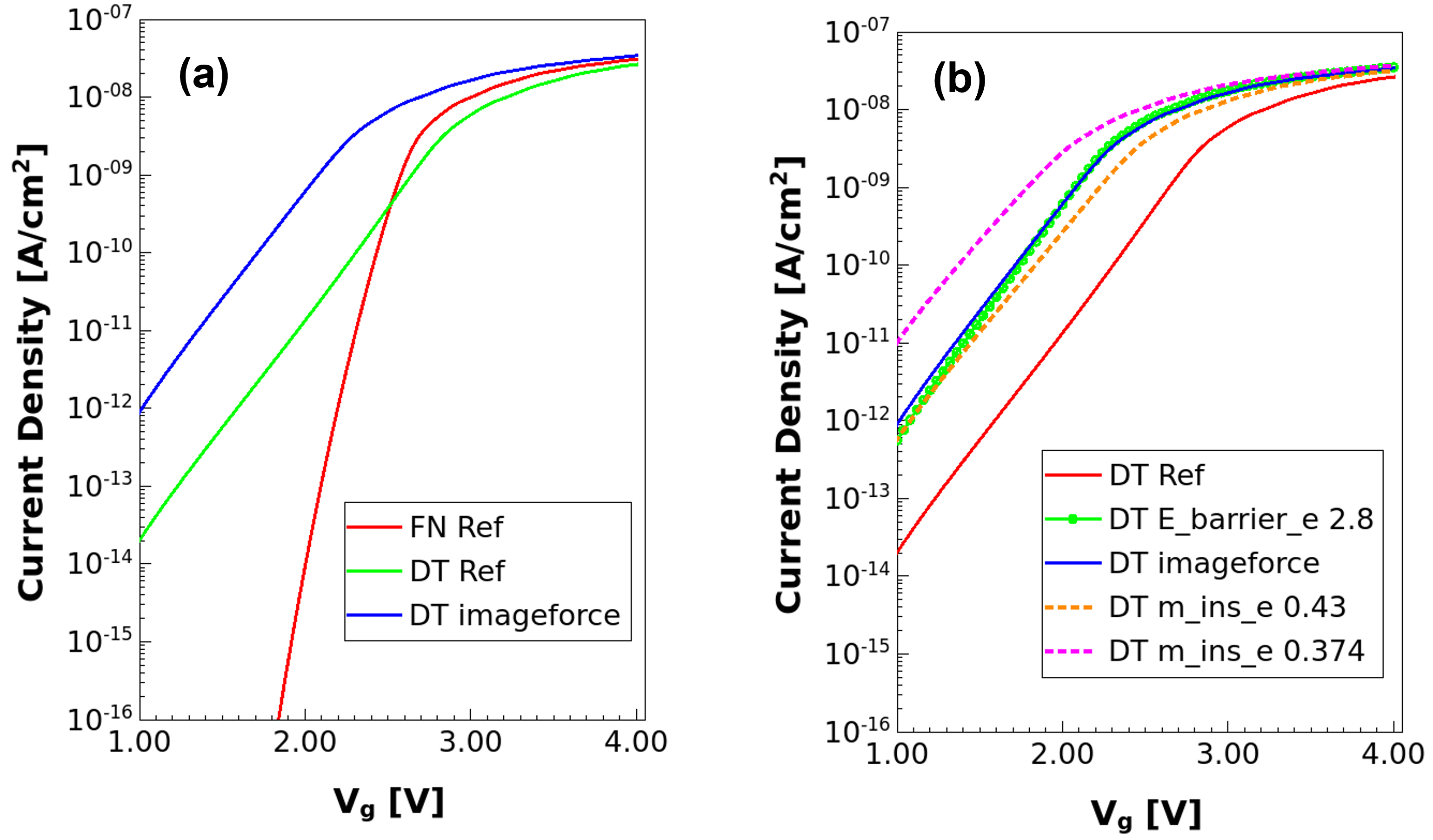
Figure 5. (Left) Comparison of direct tunneling current with Fowler–Nordheim tunneling. For DT Ref, the default parameter set is used. For DT imageforce, the barrier lowering option is activated. (Right) Effect of various DirectTunneling parameters on tunneling current. (Click image for full-size view.)
Including the image force effect degrades the simulation time and convergence. For most purposes, the effect can be approximated by reducing the overall barrier height as shown in Figure 5 (right), where E_barrier for electrons is reduced from 3.15 eV to 2.8 eV for DT E_barrier.
The insulator effective mass m_ins is another important parameter that depends on process or material quality and can be used as a calibration parameter. Figure 5 (right) shows the effect of varying m_ins on the tunneling current.
The direct tunneling current can be visualized (see Figure 6) by specifying the keywords eSchenkTunnel or hSchenkTunnel in the Plot section:
Plot {
   ...
   eSchenkTunnel hSchenkTunnel
}
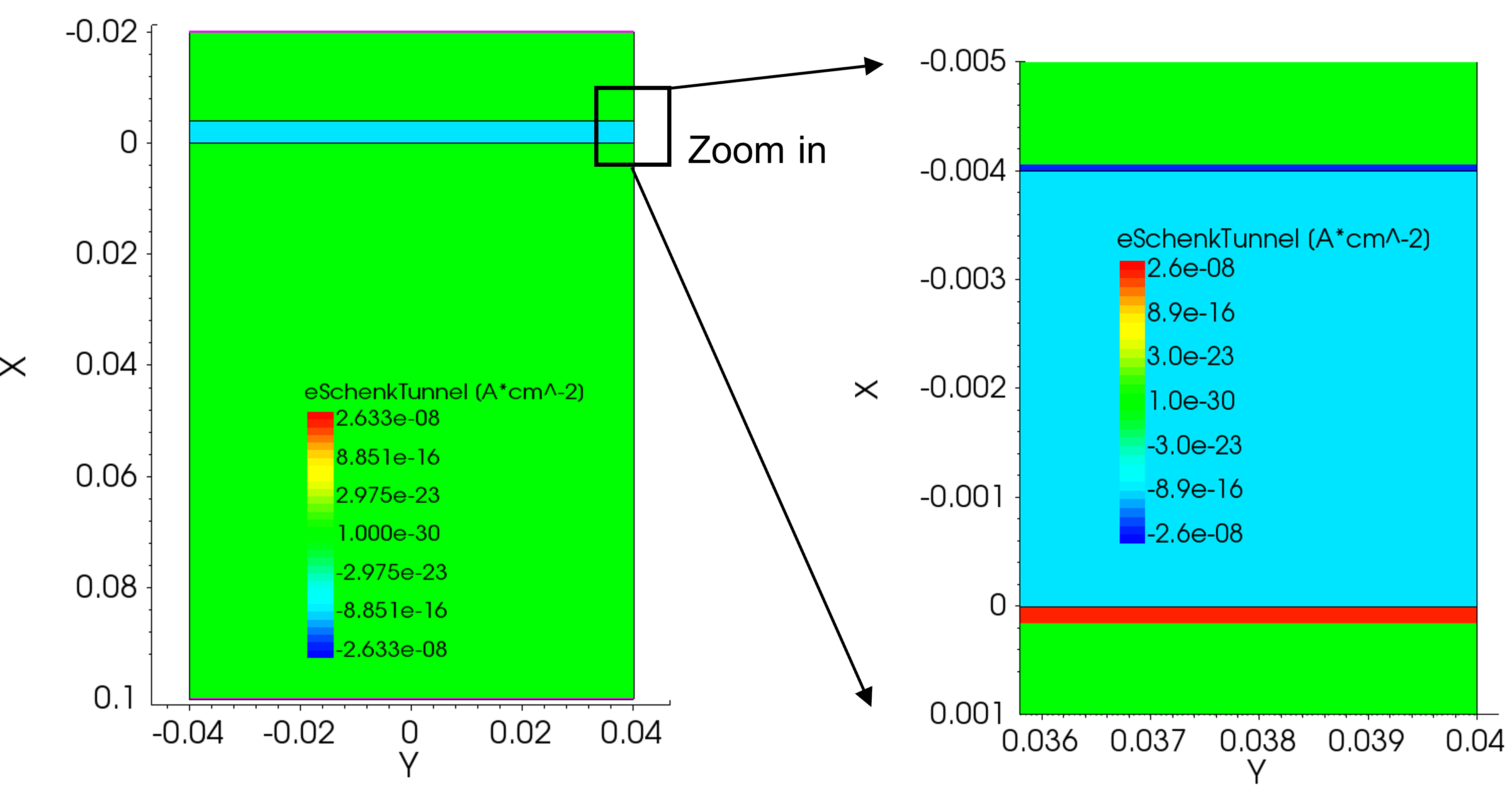
Figure 6. Visualization of direct tunneling current for Ref case. (Click image for full-size view.)
As noted earlier, the direct tunneling model assumes a trapezoidal barrier and this restricts the range of application to tunneling through insulators. For example, the presence of traps (and the related trapped charge) in the dielectric makes the barrier non-trapezoidal. To illustrate this point, assume a fixed charge in the middle of the oxide. Figure 7 (left) shows the change in conduction band shape when a fixed charge of 1e20 cm–3 is used in the middle of the gate oxide. The barrier is neither trapezoidal nor triangular.
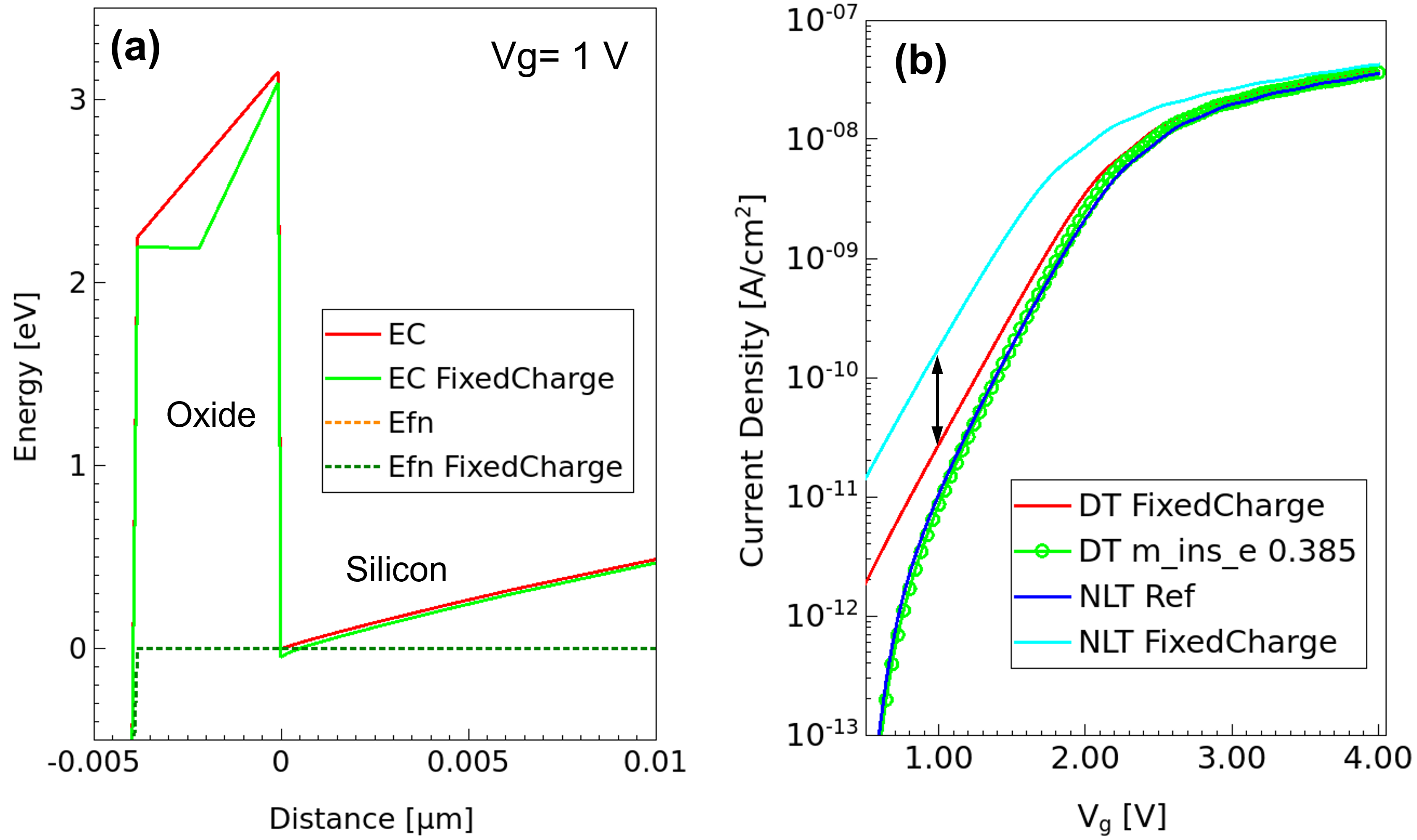
Figure 7. Trapezoidal barrier limitation of direct tunneling model. (Left) Conduction bands for the two cases, with and without fixed charge in the middle of the oxide, and (right) comparison of direct tunneling current with nonlocal tunneling current for the two cases. (Click image for full-size view.)
The nonlocal tunneling model is the most versatile model that can handle such arbitrary barrier shapes. As seen in Figure 7 (right), the nonlocal tunneling model correctly estimates approximately an order increase in the tunneling current for Vg = 1 V in the presence of the fixed charge.
One critical aspect of using the nonlocal tunneling model is defining a special-purpose nonlocal mesh. The next section discusses nonlocal meshes and related aspects.
19.2.3 Nonlocal Mesh
Nonlocal meshes are one-dimensional special-purpose meshes that Sentaurus Device needs to implement in one-dimensional, nonlocal physical models.
Specifying Nonlocal Meshes: You specify nonlocal meshes using the keyword Nonlocal, in the global Math section. Sentaurus Device supports two ways of specifying nonlocal meshes:
- Specify the regions and materials that form the tunneling barrier (keyword Barrier).
- Specify a reference surface (keywords RegionInterface, MaterialInterface, and Electrode).
In the following example, Sentaurus Device constructs a nonlocal mesh named NLM_B that consists of lines that connect the different sides of the region r.box:
Math {
   ...
   NonLocal "NLM_B" ( Barrier="r.ox" )
}
The Barrier specification is simpler but less general, and it is only suitable for nonlocal meshes used for direct tunneling through barriers that are assumed to be insulating.
Specifying a reference surface is a more general way of specifying a nonlocal mesh. In the following example, Sentaurus Device constructs a nonlocal mesh named NLM_top that consists of nonlocal lines for semiconductor vertices up to a distance of 8e-7 cm (8 nm) from the region interface r.polysi/r.ox:
Math {
   ...
   NonLocal "NLM_top" (
      RegionInterface="r.polysi/r.ox"
      Length= 8e-7
   )
}
The following specification yields the same nonlocal mesh NLM_top using a material interface instead of a region interface:
Math {
   ...
   NonLocal "NLM_top" (
      MaterialInterface="PolySi/Oxide"
      Length= 8e-7
   )
}
Verifying a Nonlocal Mesh: To facilitate verification of the constructed nonlocal mesh, Sentaurus Device writes two vector fields (NonLocalDirection and NonLocalBackDirection) to the plot file, which represent the nonlocal meshes constructed in the device. To visualize the nonlocal vectors, use the keyword NonLocal in the Plot section:
Plot {
   ...
   NonLocal
}
You will understand these aspects by using some examples. The simulations discussed here correspond to the Sentaurus Workbench parameter model=NLM. Figure 8 shows the nonlocal vectors for the nonlocal mesh NLM_top defined earlier in this section (Ref2 case). The magnified view (middle) shows two NonLocalDirection vectors corresponding to two nonlocal mesh lines "up" and "down". The head for both of these vectors points to the region interface r.polysi/r.ox (as specified in NLM_top). The length of these vectors (that is, the length of nonlocal mesh lines) is controlled by the Length option of the NLM_top specification. The tail of each vector lies on a vertex of the normal mesh (see Figure 9). The magnified view (right) shows two NonLocalBackDirection vector fields corresponding to the two nonlocal mesh lines "up" and "down". While the head of the NonLocalDirection vector represents one end of a nonlocal line, the NonLocalBackDirection vector field determines the other end of the nonlocal line.
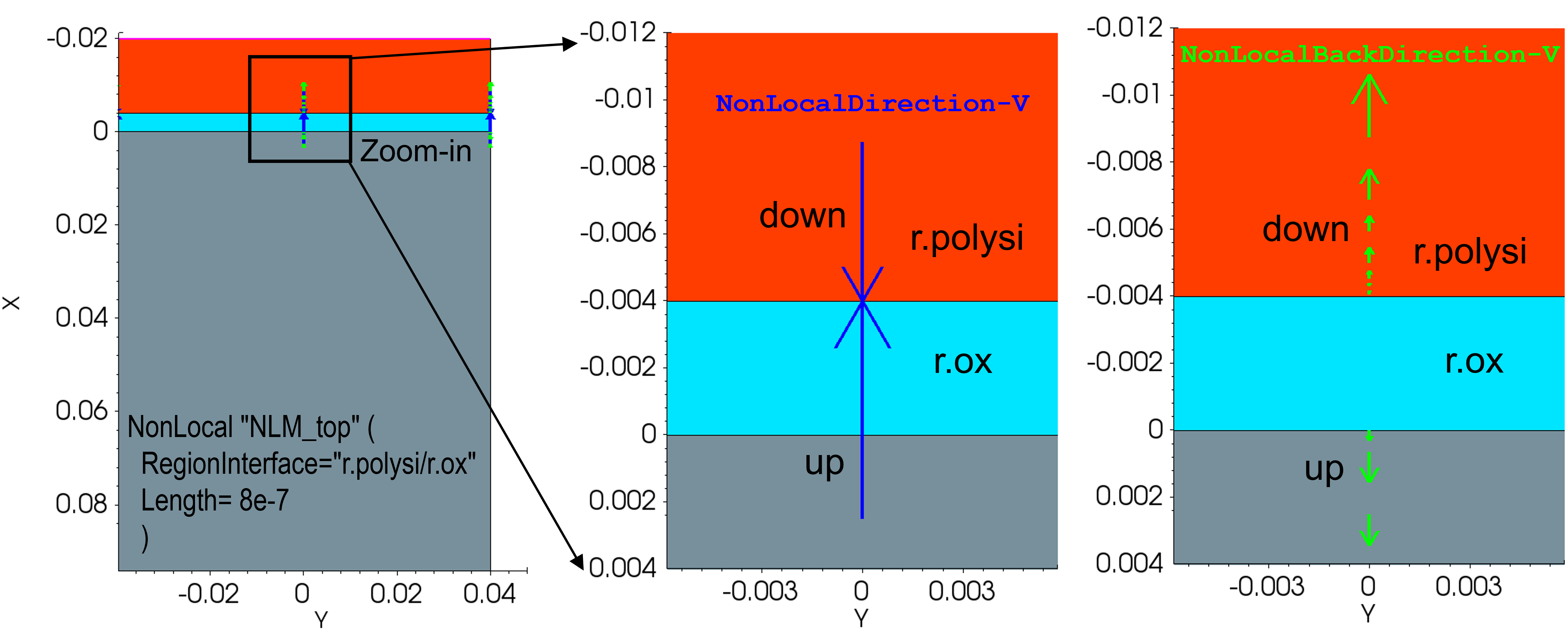
Figure 8. Nonlocal vectors corresponding to nonlocal mesh NLM_top. Magnified views (middle and right) reveal the NonLocalDirection and NonLocalBackDirection vector fields. (Click image for full-size view.)
Visualizing Data Defined on Nonlocal Mesh: You can visualize data defined on nonlocal meshes by specifying the NonLocalPlot file name in the File section and by specifying NonLocalPlot at the top level of the command file section as shown here. Sentaurus Device selects nonlocal lines close to the coordinates specified in parentheses next to NonLocalPlot keyword:
File {
   ...
   NonLocalPlot= "n@node@_nl"
}

NonLocalPlot ( (-0.006 0) (0.002 0) ) {
   eDensity
   hDensity
   ConductionBandEnergy
   ValenceBandEnergy
   eQuasiFermiEnergy
   ElectrostaticPotential
}
This feature can be used to further verify or understand the constructed nonlocal mesh NLM_top. Figure 9 shows the nonlocal plots for "down" (in the middle, for (-0.006,0)) and "up" (on the right, for (0.002,0)) nonlocal lines. Each nonlocal line is subdivided by nonlocal mesh points, to allow for the discretization of the equations that constitute the physical models. Sentaurus Device performs this subdivision automatically to obtain optimal interpolation between the nonlocal mesh and the normal mesh. For example, from Figure 9, you can see that Sentaurus Device adds two new mesh points p4 and p5 in silicon for the nonlocal mesh, in addition to p1, p2, and p3 normal mesh points.
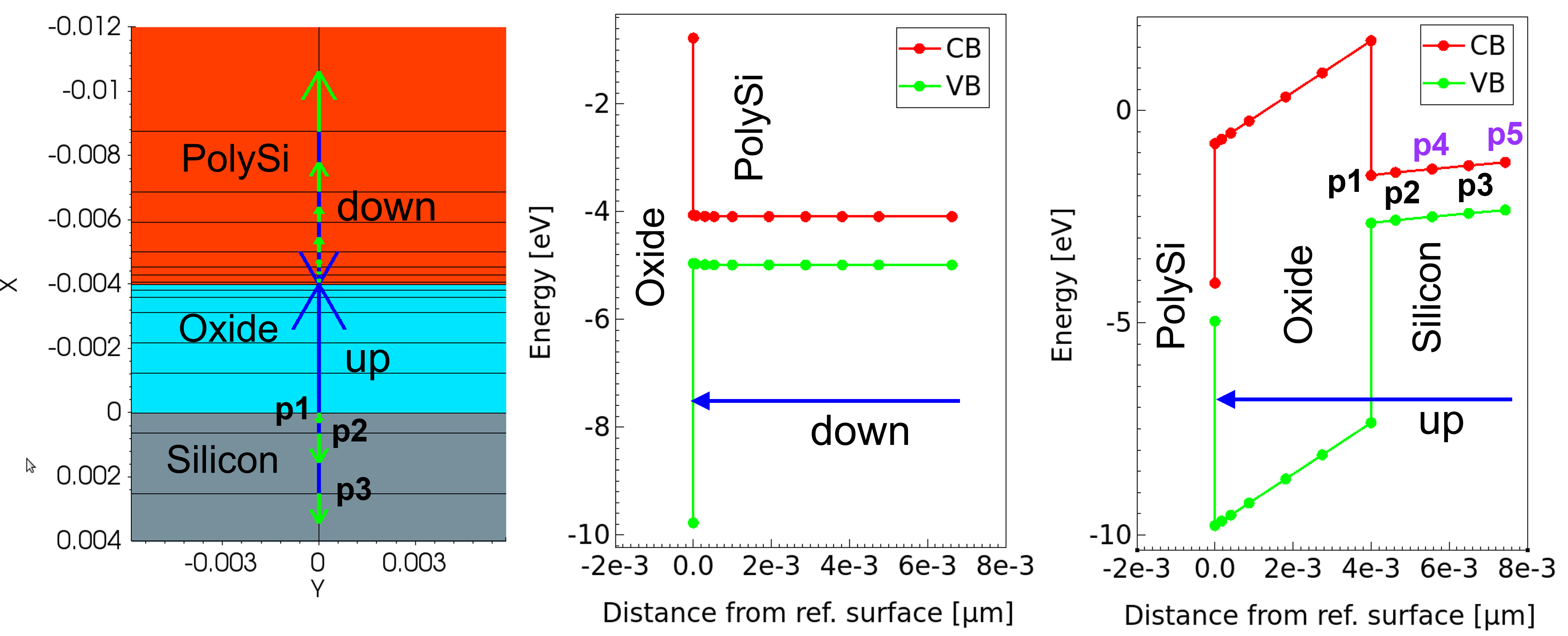
Figure 9. Structure showing normal mesh and nonlocal vectors corresponding to the nonlocal mesh NLM_top. The nonlocal plots for "down" (middle) and "up" (right) nonlocal lines. (Click image for full-size view.)
As seen for the Ref2 case, Sentaurus Device constructs two nonlocal mesh lines "up" and "down" for NLM_top, which might not be the intended behavior. This is because, by default, Sentaurus Device constructs nonlocal lines that end in semiconductor regions (both Silicon and PolySi). Sentaurus Device provides various options to override the default behavior and to further control the construction of the nonlocal mesh.
Controlling a Nonlocal Mesh: The parameter Length of Nonlocal determines the maximum distance of the normal mesh vertex to the reference surface (in centimeters). Endpoint is another important option. The default is Endpoint (allowing for the construction of a nonlocal mesh) for semiconductor regions and -Endpoint (restricts the construction of a nonlocal mesh) for insulator regions.
You can redefine NLM_top with the -Endpoint option for the Ref case in order to restrict the nonlocal mesh ("down") ending in PolySi. Figure 10 shows the resulting nonlocal mesh.
Math {
   ...
   NonLocal "NLM_top" (
      RegionInterface="r.polysi/r.ox"
      Length= 8e-7
      -Endpoint(Material="PolySi")
   )
}
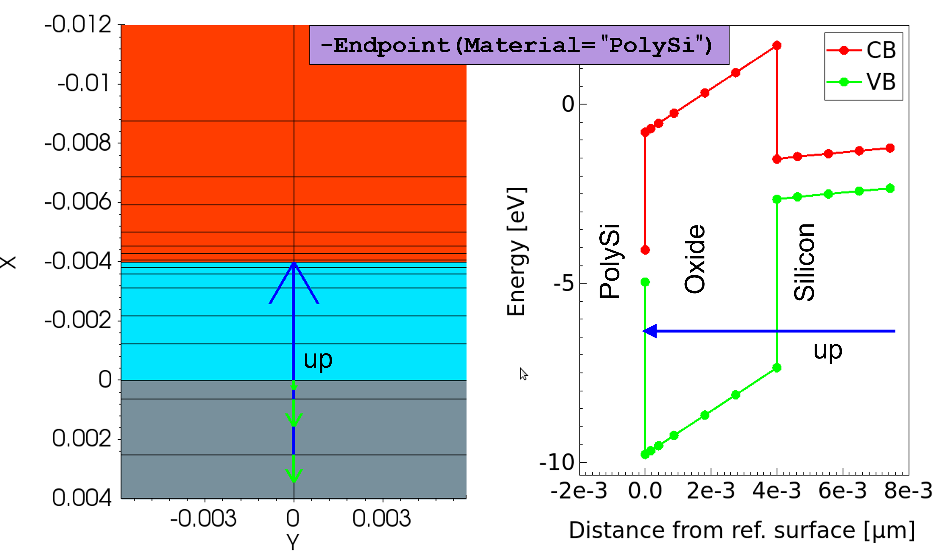
Figure 10. Using Endpoint in nonlocal mesh construction. (Click image for full-size view.)
The parameter Permeation of Nonlocal extends the nonlocal line beyond the reference surface by a value specified by Permeation. Now, you redefine NLM_top with the Permeation option for the Permeation case as shown here:
Math {
   ...
   NonLocal "NLM_top" (
      RegionInterface="r.polysi/r.ox"
      Length= 8e-7
      -Endpoint(Material="PolySi")
      Permeation=2e-7
   )
}
Figure 11 shows the resulting nonlocal mesh.
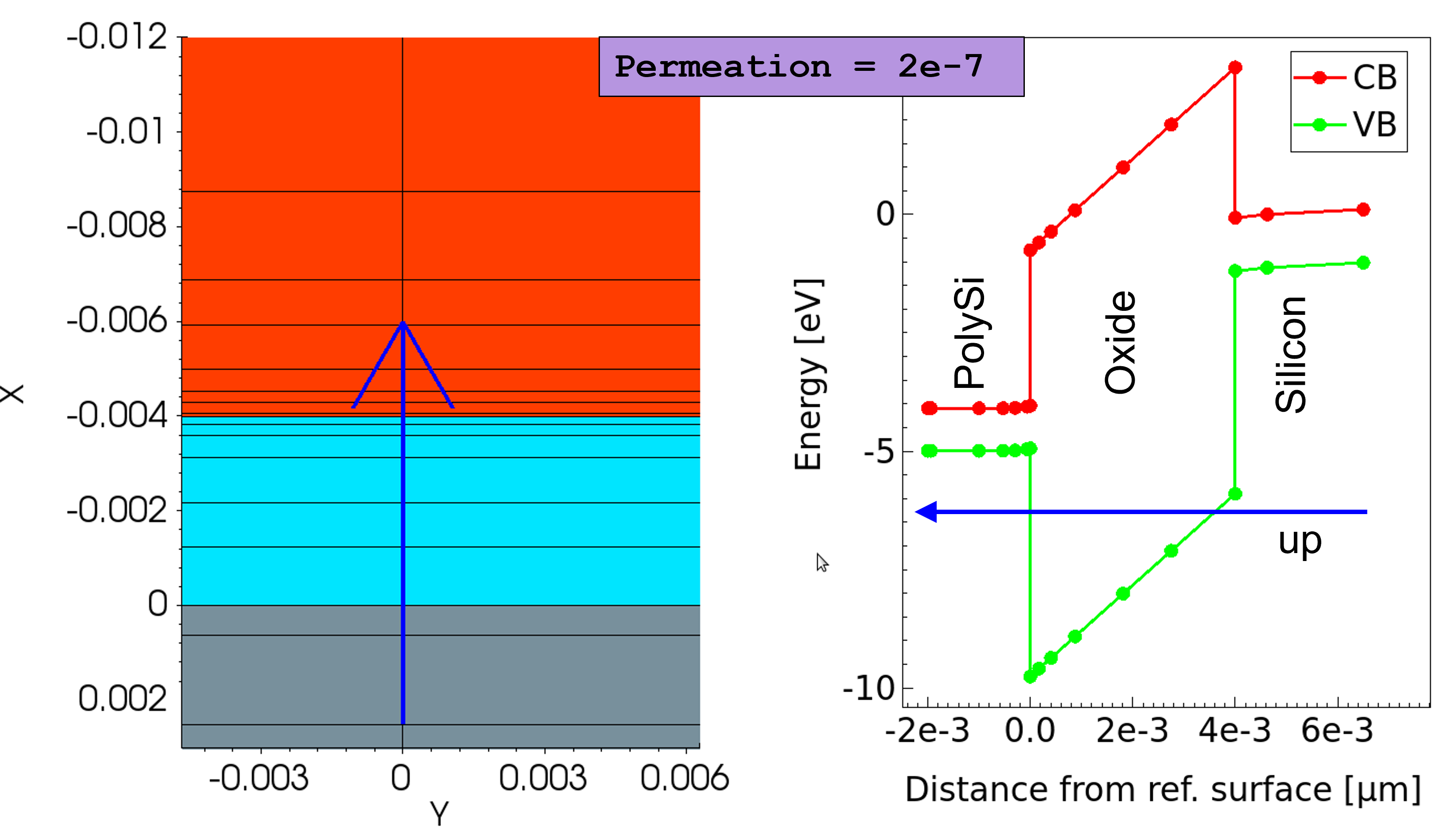
Figure 11. Using Permeation in nonlocal mesh construction. (Click image for full-size view.)
The Sentaurus Workbench parameter mesh_fac is used to modify the normal mesh, which allows you to study the effect a normal mesh has on a nonlocal mesh. Figure 12 shows that the dense normal mesh (mesh_fac=0.4) results in dense nonlocal line points.
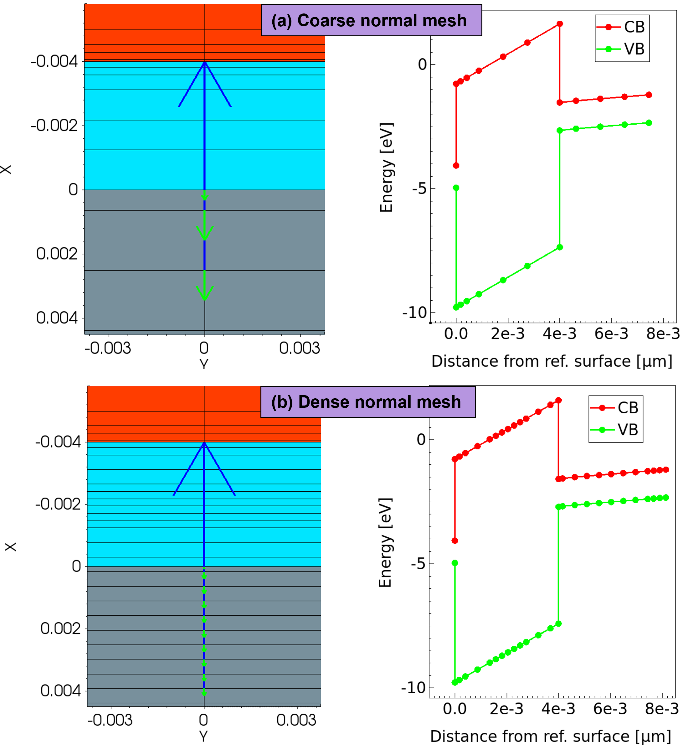
Figure 12. Dependence of nonlocal mesh on normal mesh. (Click image for full-size view.)
19.2.4 Nonlocal Tunneling Model
The nonlocal tunneling model includes the following features:
- Handles arbitrary barrier shapes (band edge profile is computed by solving the transport equations and the Poisson equation along a special-purpose nonlocal mesh)
- Provides different approximations for the tunneling probability: WKB (default) and Schroedinger
- Allows tunneling between the valence band and conduction band (Band2Band, optional) in addition to tunneling between conduction band and conduction band (see Figure 13)
- Includes quantization corrections to tunneling with the density gradient model
- Includes carrier heating terms (PeltierHeat, optional) with hydrodynamic simulations
Model and Related Parameters: The key feature of the nonlocal tunneling model is that the tunneling current through the barrier is converted into a local generation or recombination process. The tunneling current is estimated as the integral over the net recombination rate. Figure 13 shows various tunneling current contributions for a poly-Si, oxide, and silicon (semiconductor–insulator–semiconductor) structure. The model supports the band-to-band tunneling contributions, jcv and jvc in addition to jcc and jvv.
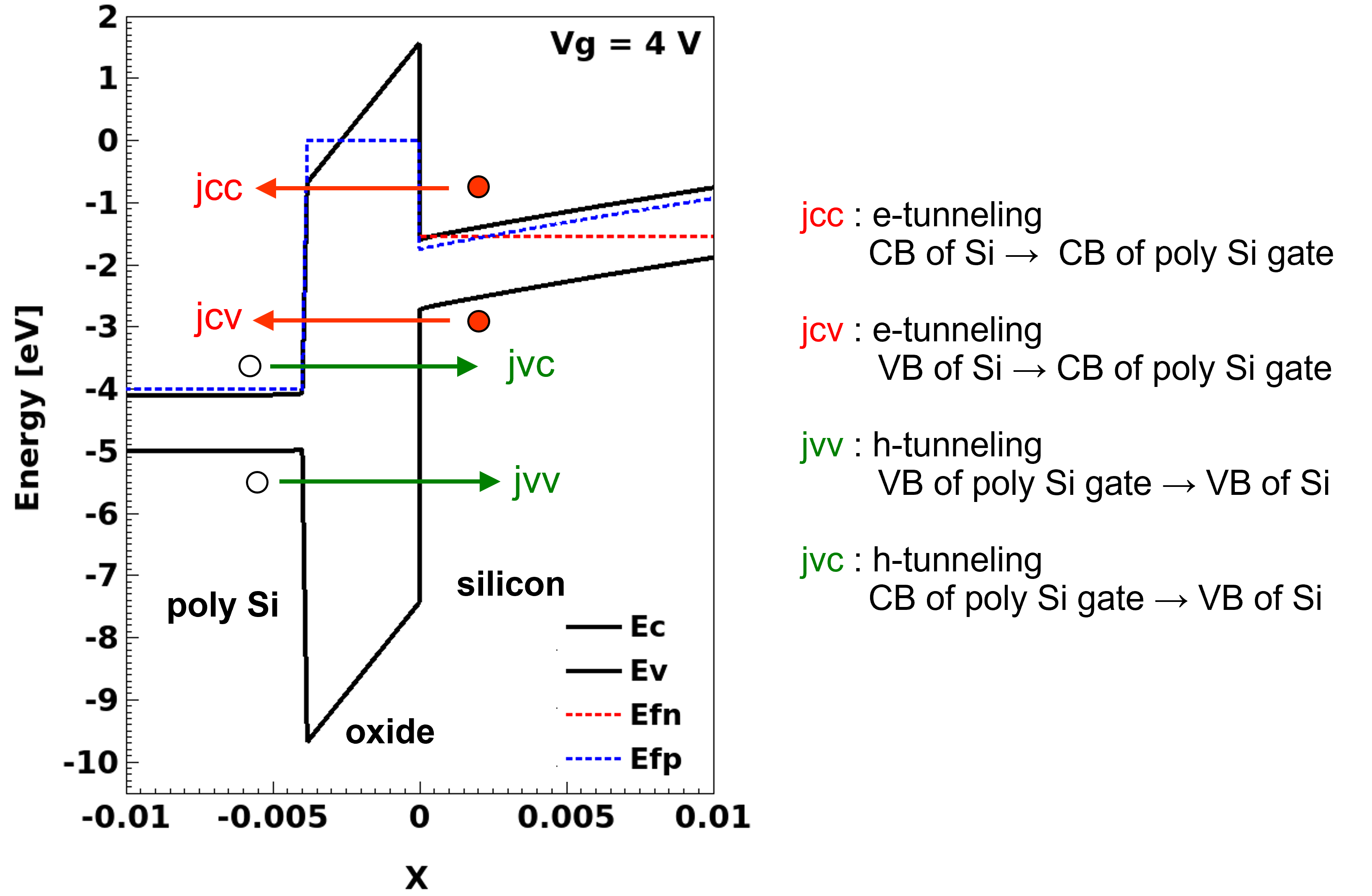
Figure 13. Four contributions to total tunneling current: electron tunneling (jcc, jcv) and hole tunneling (jvv, jvc) components. (Click image for full-size view.)
The following expressions give the contribution to the electron tunneling current density (eBarrierTunneling, jCC) by electrons that tunnel from the conduction band to the conduction band.
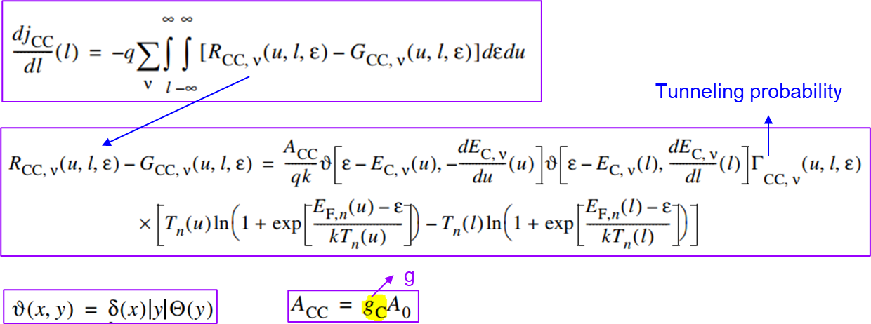
The following expressions give the contribution to the electron tunneling current density (eBarrierTunneling, jCV) by electrons that tunnel from the conduction band to the valence band for Band2Band=Simple. With Band2Band=Simple, the net eBarrierTunneling current equals jcc+jcv.
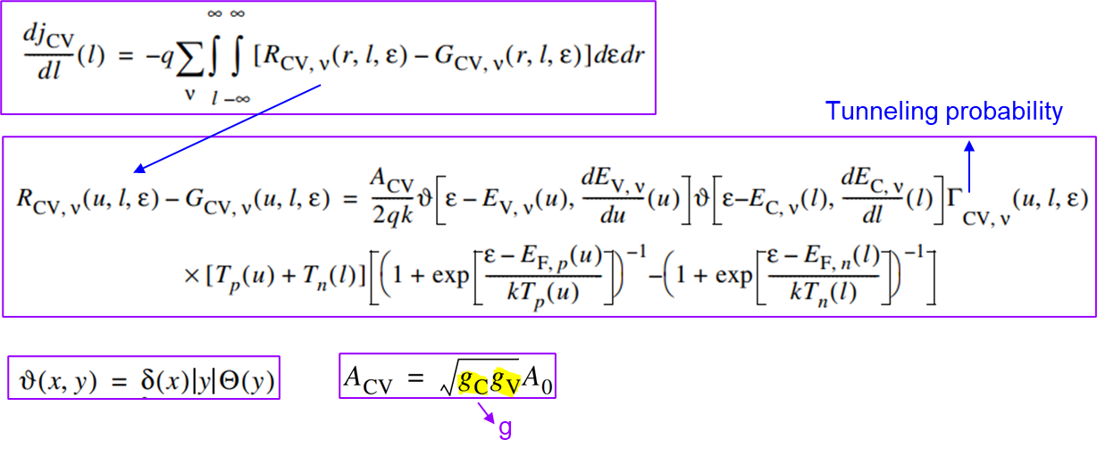
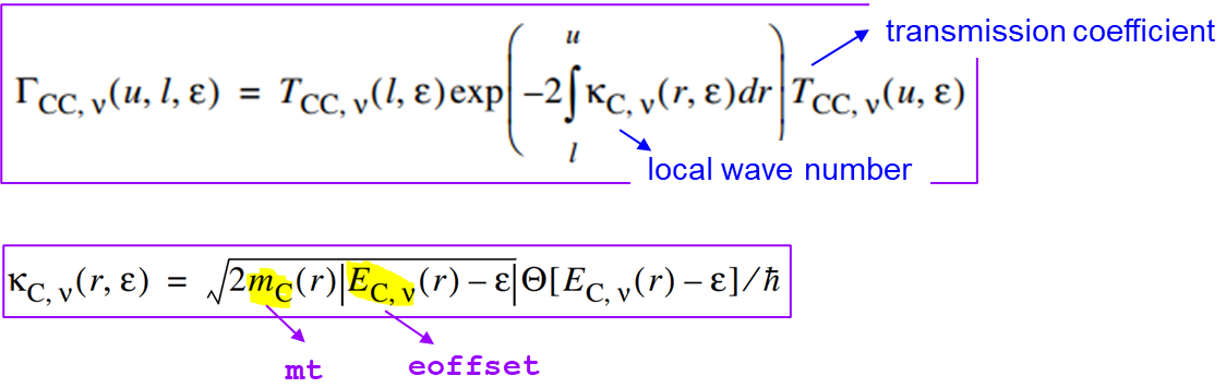
The tunneling probabilities noted above are, by default, based on the WKB approximation and are given by the following expressions:
If the Transmission keyword is not set to eBarrierTunneling, then by default the interface transmission coefficients equal 1: \( T_{\text"CC,v"}\=T_{\text"VV,v"}\=1 \)
As noted, the previous expressions are for eBarrierTunneling. Analogous expressions hold for hBarrierTunneling.
Usage: The nonlocal tunneling model is activated and controlled in the global Physics section. The following syntax switches on electron tunneling (the jCC component shown in Figure 13) for the nonlocal mesh named NLM_top:
Physics {
   ...
   eBarrierTunneling "NLM_top"
}
To invoke the band-to-band tunneling jcv in addition to jcc, you must specify the keyword Band2Band as an option to eBarrierTunneling as shown here (the total current then equals jcc + jcv):
Physics {
   ...
   eBarrierTunneling "NLM_top" (Band2Band=Full)
}
The parameter pair mt determines the tunneling masses \( m_C \) and \( m_V \). The parameter pair g determines the dimensionless prefactors \( g_C \) and \( g_V \) and is an optional parameter. The parameters can be specified globally as shown here (the values mentioned for the parameter pair g are the default parameters):
BarrierTunneling
{
   mt	= 0.4 ,	0.32
   g	= 2.1 ,	0.66
}
The specification of nonzero mt values is mandatory as Sentaurus Device does not assume any default values.
The parameters can also be specified in region-specific or material-specific parameter sets. For example:
Material= "Oxide" {
   BarrierTunneling
   {
   mt	= 0.4 ,	0.32	# [1]
   }
}
Material= "Silicon" {
   BarrierTunneling
   {
   mt	= 0.19 , 0.16	# [1]
   }
}
Material= "PolySi" {
   BarrierTunneling
   {
   mt	= 0.19 , 0.16	# [1]
   }
}
The nonlocal mesh (NLM_top) is defined in the Math section of the command file as previously mentioned. To understand the tunneling current contributions, various simulation cases as shown in Table 1 are considered.
| Simulation case | Keyword | Description |
|---|---|---|
| eBarr | eBarrierTunneling | jcc |
| eBarr_B2BFull | eBarrierTunneling(Band2Band=Full) | jcc+jcv |
| hBarr | hBarrierTunneling | jvv |
| hBarr_B2BFull | hBarrierTunneling(Band2Band=Full) | jvv+jvc |
| B2BFull | eBarrierTunneling(Band2Band=Full) hBarrierTunneling(Band2Band=Full) | jvv+jvc+jvv+jvc |
Figure 14 shows the tunneling current for various simulation cases. Figure 15 shows the band diagrams at -4, 0, and 4 V, noting the dominant current contributions. For positive gate voltages, up to Vg ≅ 1 V, electron tunneling from the conduction band of silicon to the conduction band of poly-Si (jcc) is the dominant current component (see Figure 15 (left). From Vg ≥ 1 V, the band bending (see Figure 15 (right) favors the tunneling of electrons from the valence band of silicon to the conduction band of poly-Si (jcv) and is the dominant current component for Vg ≥ 1 V.
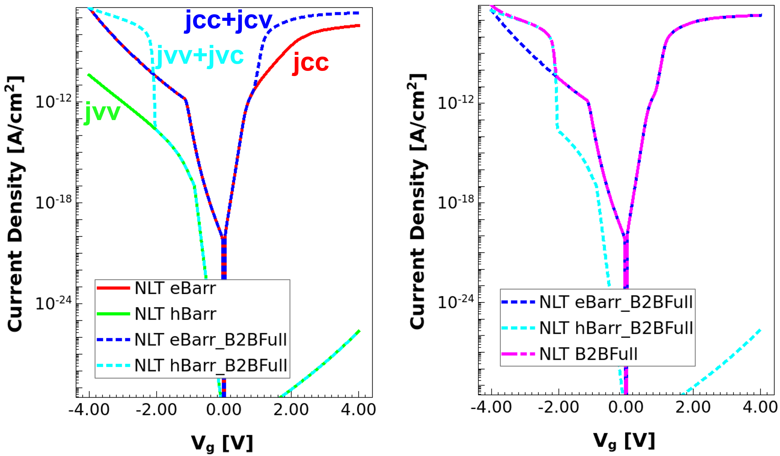
Figure 14. Various tunneling current contributions. (Click image for full-size view.)
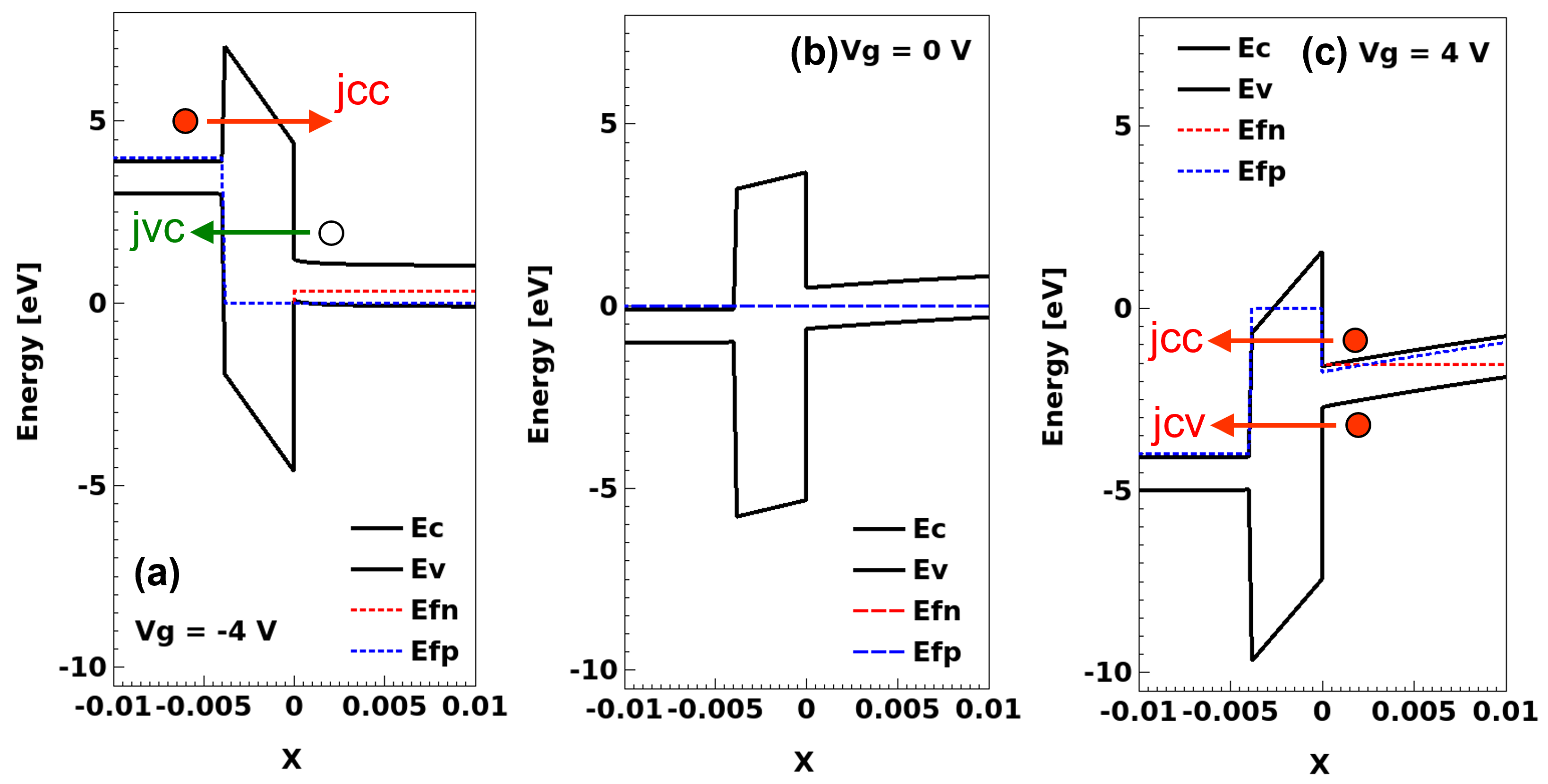
Figure 15. Dominant tunneling current contributions in forward bias and reverse bias. (Click image for full-size view.)
For negative gate voltages, up to Vg ≅ -2 V, the electron tunneling from the conduction band of poly-Si to the conduction band of silicon (jcc) is the dominant current component. However, it can be seen that jvv (h-tunneling from the valence band of silicon to the valence band of poly-Si) is much more pronounced for negative gate voltages compared to positive gate voltages. For Vg ≤ -2 V, the band bending (see Figure 15 (left) favors the tunneling of holes from the conduction band of silicon to the valence band of poly-Si (jvc) and is the dominant current component for Vg ≤ -2 V.
The keywords eBarrierTunneling and hBarrierTunneling in the Plot section facilitate the visualization of the carrier generation rates due to nonlocal tunneling. Negative values represent the disappearance of carriers, and positive values represent the generation of carriers due to the tunneling process. Figure 16 shows the electron (eBarrierTunneling) and hole (hBarrierTunneling) tunneling generation rates for the eBarr (jcc) and eBarr_B2BFull (jcc+jcv) cases at Vg=4 V.
Plot {
   ...
   eBarrierTunneling hBarrierTunneling
}
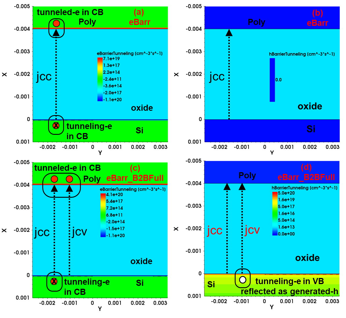
Figure 16. Carrier tunneling generation rates for eBarr and eBarr_B2BFull. (Click image for full-size view.)
For eBarr, electrons tunnel from the conduction band of silicon to the conduction band of polysilicon. This is represented by the disappearance of electrons (eBarrierTunneling=-1.1e20) at the silicon–oxide interface and the generation of electrons (eBarrierTunneling=7.1e19) at the polysilicon–oxide interface.
For eBarr_B2BFull, electrons tunnel to the conduction band of polysilicon not only from the conduction band of silicon (jcc) but also from the valence band of silicon (jcv). This is reflected by a much higher eBarrierTunneling (4.1e20) compared to the eBarr case (7.1e19). Furthermore, the tunneling of electrons from the valence band of silicon also results in hole generation (hBarrierTunneling=5e20) in silicon.
The tunneling mass of oxide is one of the key parameters used for the calibration of the gate current. Figure 17 shows the effect of the tunneling mass of oxide on the tunneling current for eBarr_B2BFull.
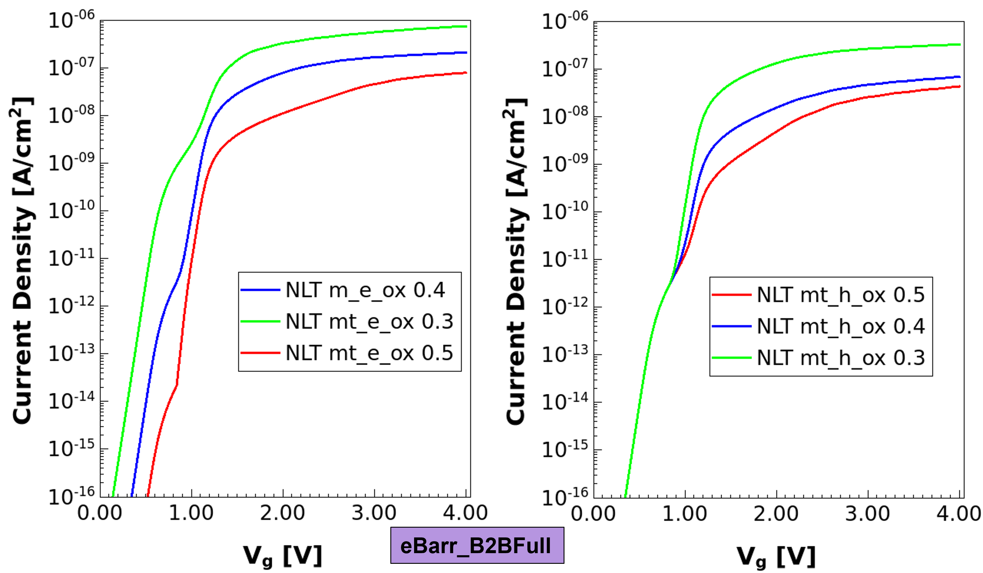
Figure 17. Effect of tunneling mass of oxide on tunneling current for eBarr_B2BFull. (Click image for full-size view.)
19.2.5 Nonlocal Tunneling for Traps (Trap-Assisted Tunneling)
Traps play a key role in device physics. Traps (and related trap-assisted tunneling) increase gate leakage currents in MOSFETs. Traps have a vital role in charge-trap-based memory devices. For an introduction to various aspects related to traps, see Section 13. Special Focus: Traps.
This section initially examines the models for trap-assisted tunneling and then uses the same for estimating gate leakage in a MOS structure.
Trap charges are computed by multiplying the trap occupation by the trap concentration. Trap occupation is independent of the trap concentration and depends on the Fermi level and trap energy together with various capture or emission rates, corresponding to various capture or emission processes.
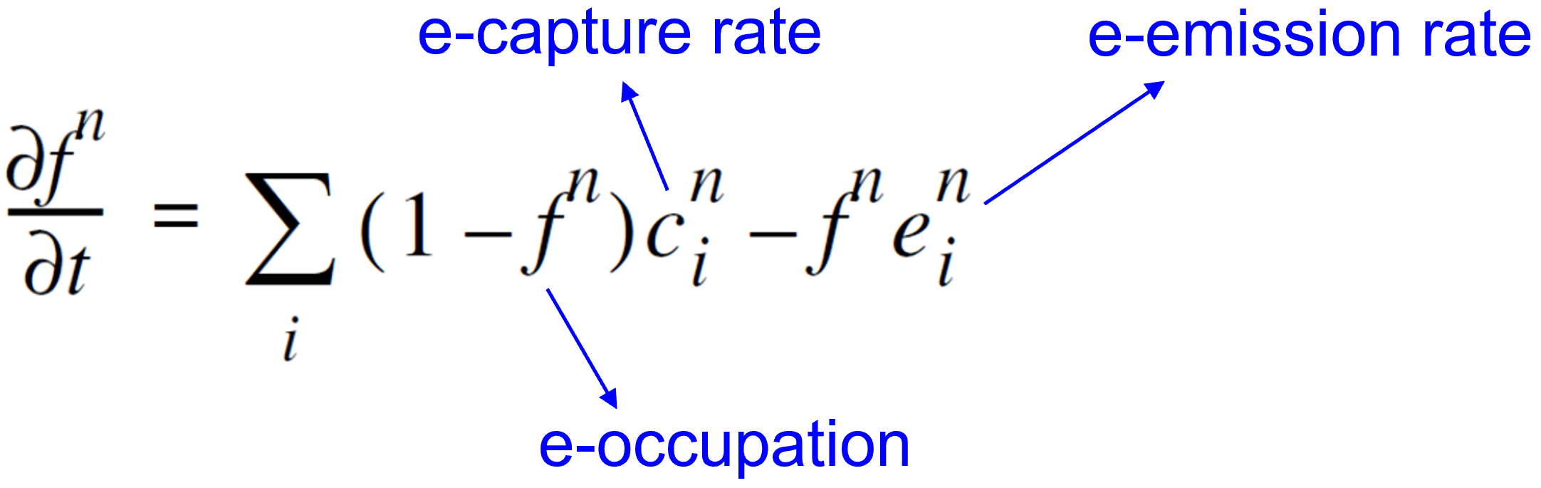
Each capture and emission process couples the trap to a reservoir of carriers. If only a single process would be effective, in the stationary state, then the trap would be in equilibrium with the reservoir for this process. This consideration (the principle of detailed balance) relates capture and emission rates:
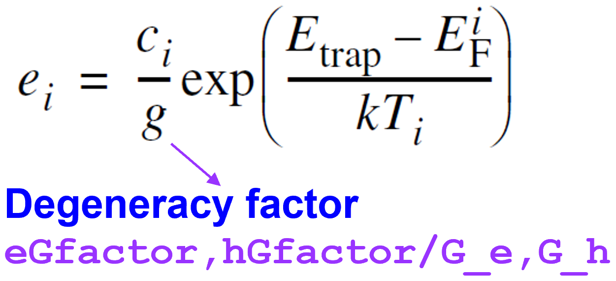
Figure 18 shows three groups of capture and emission processes typical for semiconductor devices:
- Local capture and emission
- Nonlocal elastic tunnel capture and emission (based on nonlocal mesh)
- Nonlocal inelastic phonon-assisted tunnel capture and emission (based on nonlocal mesh)
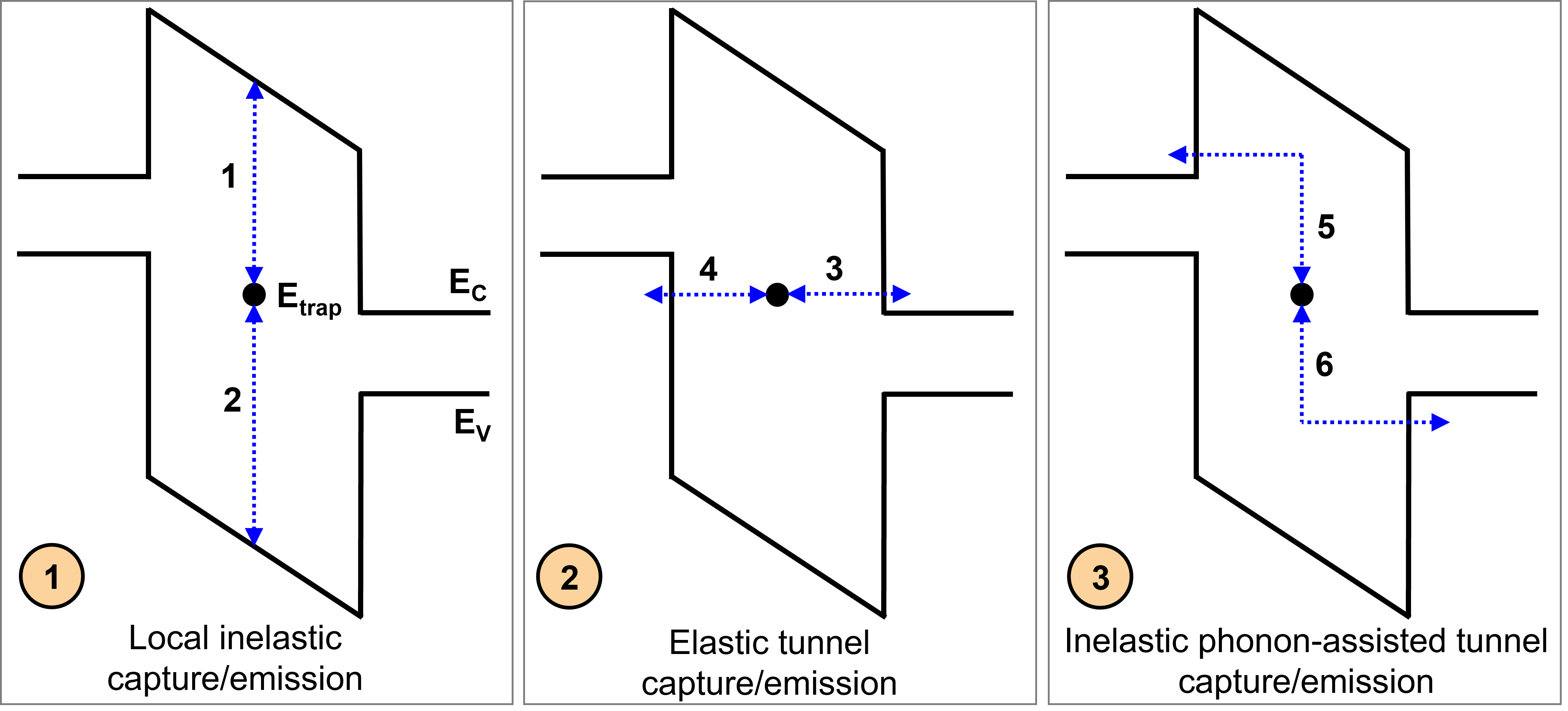
Figure 18. Different capture and emission processes. (Click image for full-size view.)
Without nonlocal tunneling for traps, only local exchange of carriers with both the bands is considered (processes 1 and 2 in Figure 18). Processes 1 and 2 are relevant only for semiconductors and not for insulators as Sentaurus Device does not solve the current continuity equations in insulators.
The following expressions summarize the model and related parameters.
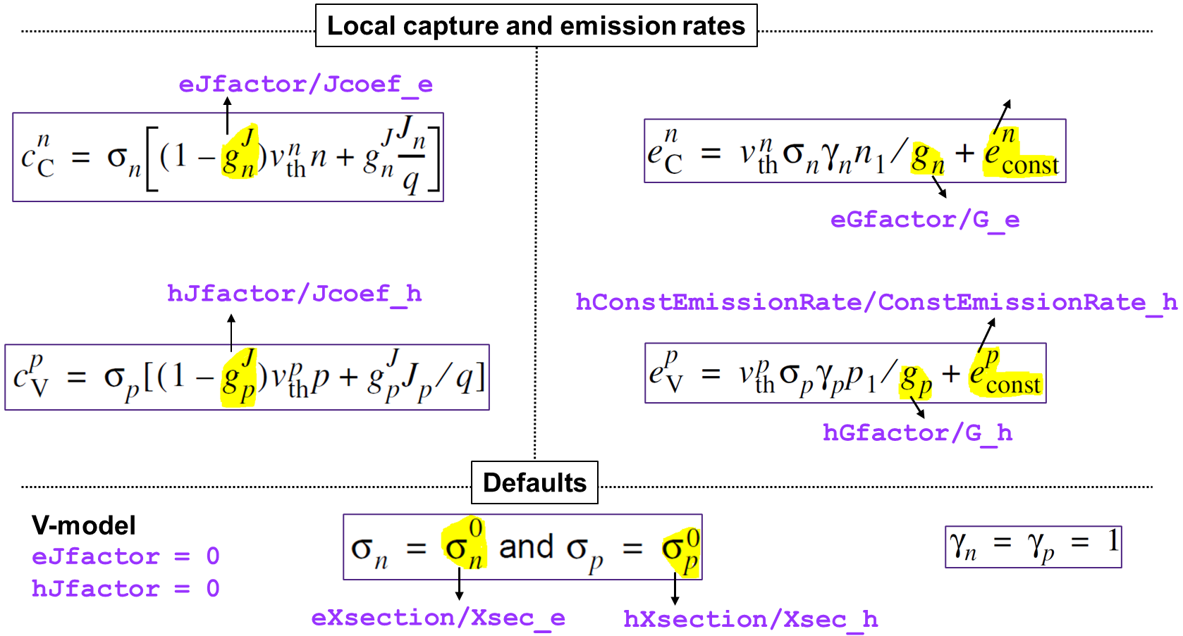
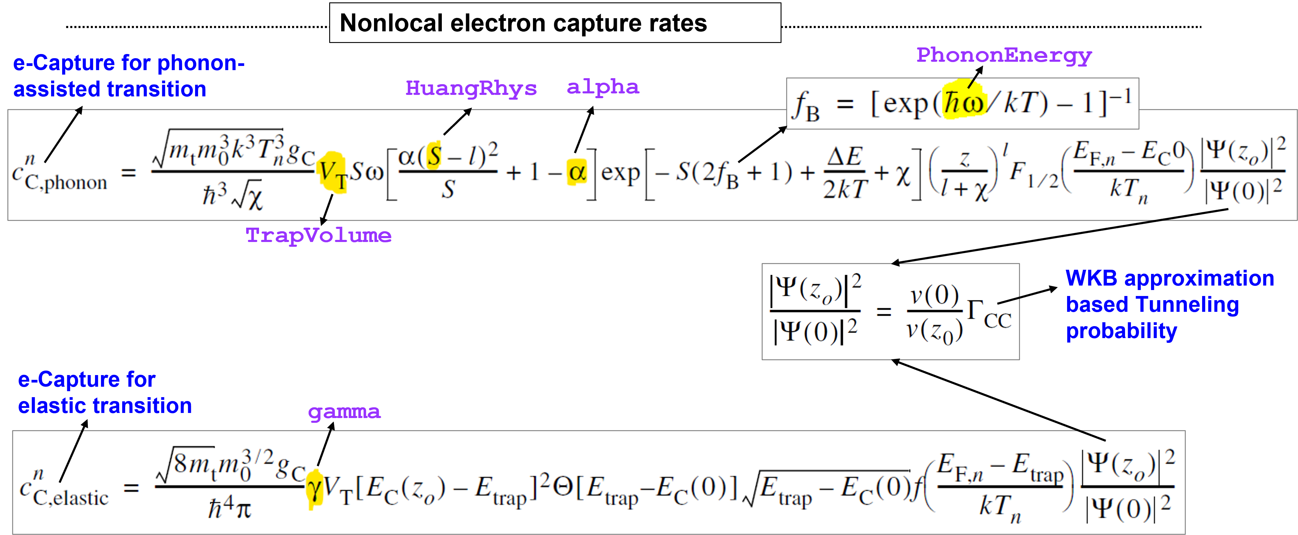
Traps can be coupled to nearby interfaces and contacts by tunneling (based on a nonlocal mesh). Sentaurus Device models nonlocal tunneling to traps as the sum of an inelastic phonon-assisted process and an elastic process. The following expressions summarize the electron capture rates for the conduction band. Similar expressions hold for holes and the valence band.
Specify TrappingRates in the Plot section to see the capture and emission rates for each trap, split into local processes (TotalLocalCapture and TotalLocalEmission), inelastic tunneling processes (TotalInelasticCapture and TotalInelasticEmission), and elastic tunneling processes (TotalElasticCapture and TotalElasticEmission).
To plot the recombination rates for the conduction band and valence band due to tunneling through traps, specify eGapStatesRecombination and hGapStatesRecombination, respectively.
Plot {
   ...
   TrappingRates
   eGapStatesRecombination hGapStatesRecombination
   ...
}
While eBarrierTunneling and hBarrierTunneling plot tunneling generation rates corresponding to nonlocal tunneling, eGapStatesRecombination and hGapStatesRecombination plot tunneling recombination rates corresponding to nonlocal tunneling for traps.
Now, you will look at the use of the model for an MOS example. The simulations used in this section correspond to model=TAT. The following syntax (case=NLM_both) defines bulk traps with a peak concentration of 1e19 cm–3 in the middle of the r.ox region. The trap concentration profile is shown in Figure 19 (left).
Physics(region="r.ox") {
   Traps(
      ( Acceptor Level EnergyMid= 1.5 FromConductionBand Conc= 1e19
        SpatialShape= Uniform SpaceMid=(-2e-3,0,0) SpaceSig=(0.4e-3,100,100)
        eBarrierTunneling(NonLocal= "NLM_top" NonLocal= "NLM_bot")
        hBarrierTunneling(NonLocal= "NLM_top" NonLocal= "NLM_bot")
        eXSection= 1e-10 hXSection= 1e-10
        TrapVolume= 1e-5
      )
   )
}
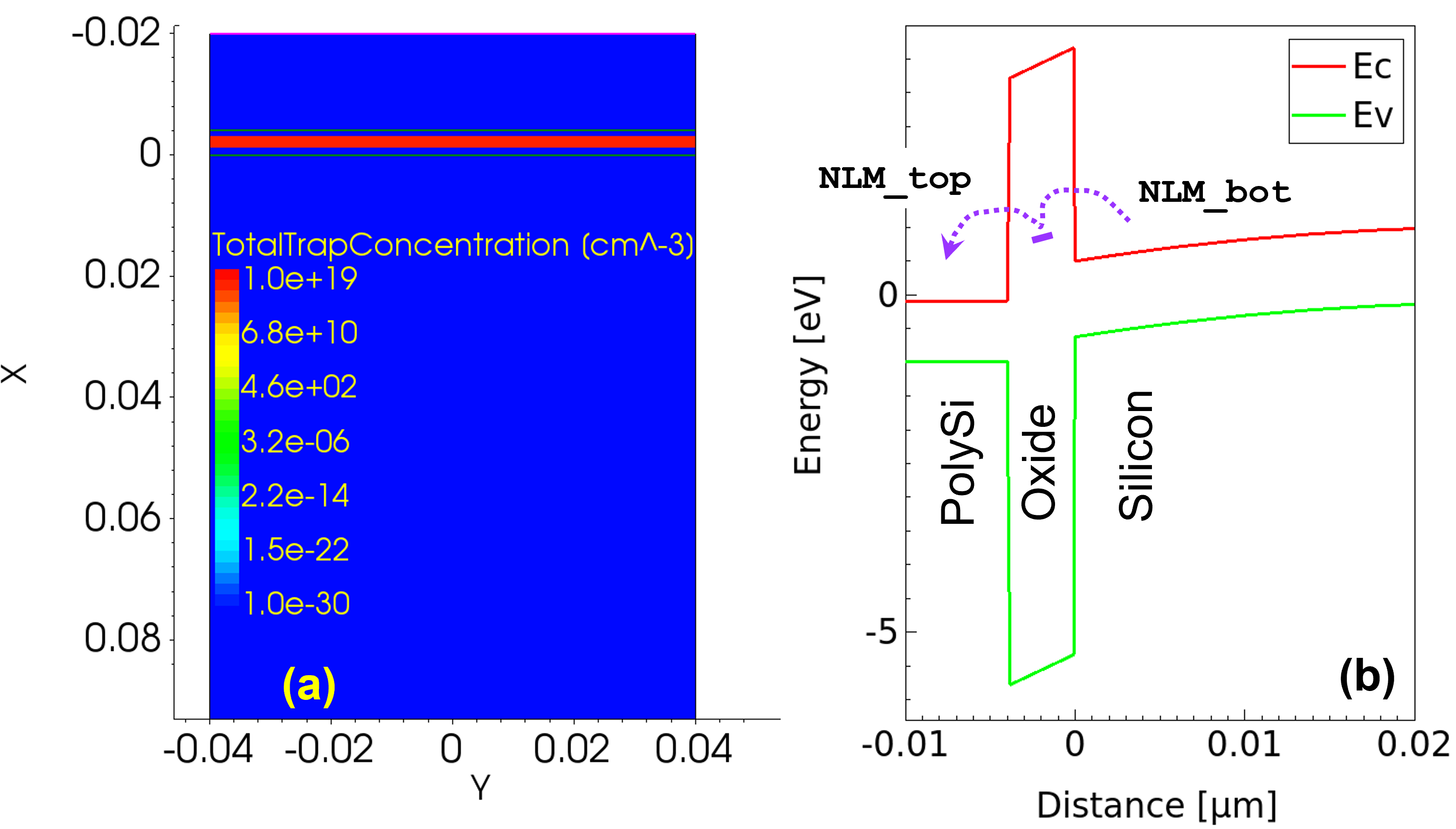
Figure 19. (Left) Trap concentration profile for case=TAT and (right) trap-assisted tunneling process and two nonlocal meshes NLM_bot and NLM_top. (Click image for full-size view.)
Nonlocal tunneling for traps (trap-assisted tunneling) requires two nonlocal meshes (NLM_bot and NLM_top defined as follows), which connect the traps to the electrode and substrate:
   NonLocal "NLM_top" (
      RegionInterface="r.polysi/r.ox"
      Length= 3e-7
      -Endpoint(Material="PolySi")
   )
   NonLocal "NLM_bot" (
      RegionInterface="r.si/r.ox"
      Length= 3e-7
      -Endpoint(Material="Silicon")
   )
For further understanding, consider three simulation cases NLM_bot, NLM_top, and NLM_both. The electron trapped charge under the gate bias of Vg=4 V is shown in Figure 20. For NLM_bot, electrons are trapped in the oxide traps and cannot tunnel further to the top electrode owing to the missing nonlocal mesh that connects the traps to the top electrode. For NLM_top, electrons are not trapped in the oxide as expected. For NLM_both, the trapped electrons tunnel further to the top electrode, thereby resulting in a trap-assisted tunneling current.
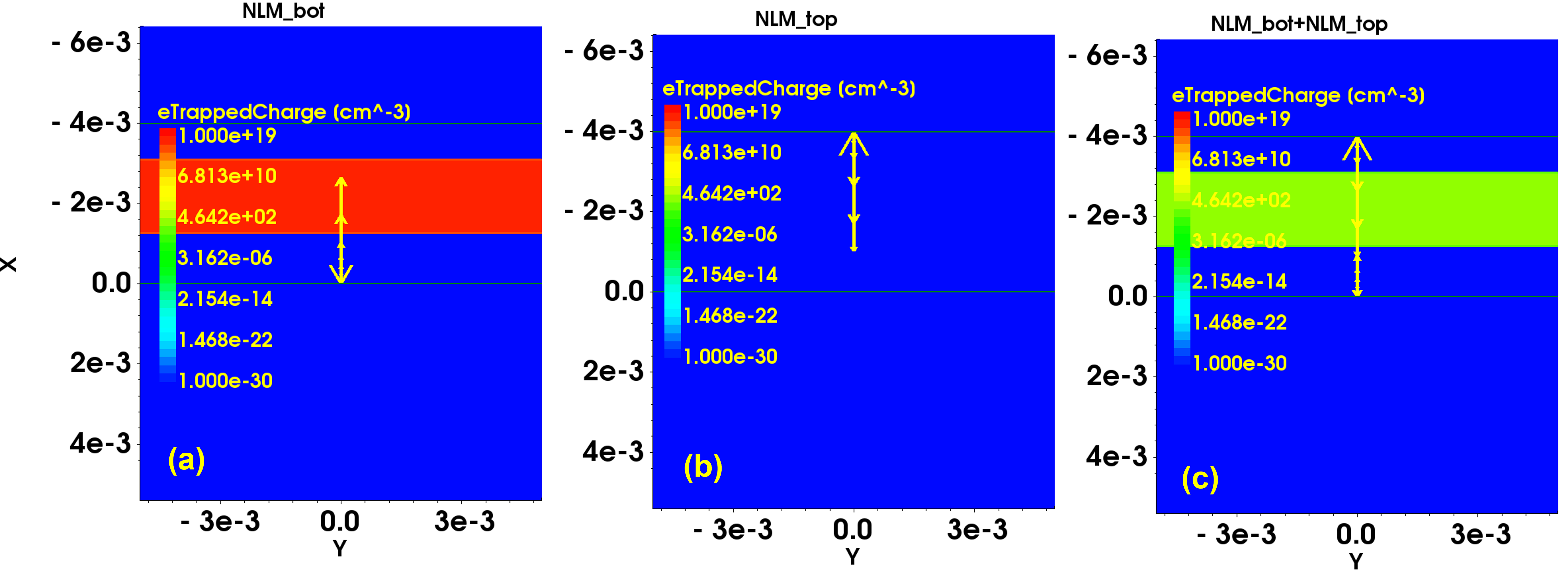
Figure 20. Three simulation cases NLM_bot, NLM_top, and NLM_both and corresponding electron trapped charge at Vg = 4 V. (Click image for full-size view.)
Figure 21 shows the effect of trap energy level and trap volume on the trap-assisted tunneling current.
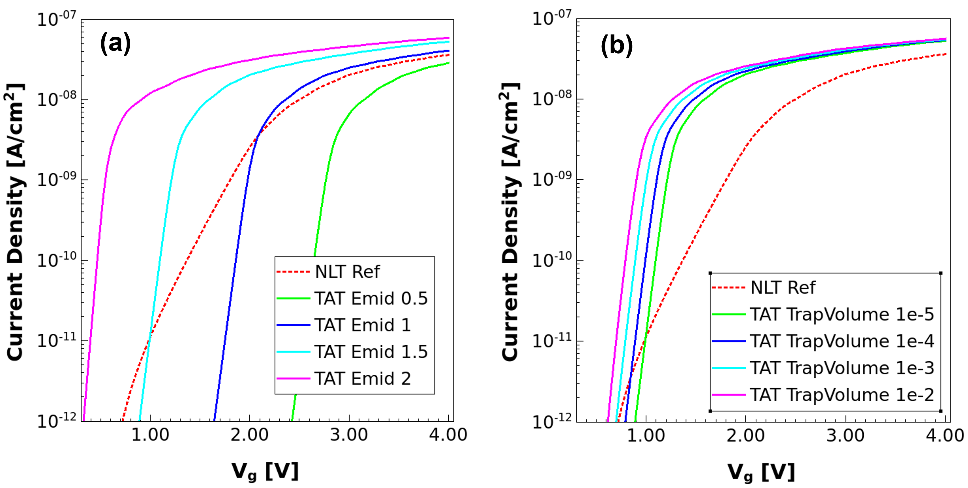
Figure 21. Effect of trap energy level and trap volume on trap-assisted tunneling current. (Click image for full-size view.)
19.3 Example: Schottky Diode
This section discusses the setup to simulate the tunneling current characteristics of a GaN Schottky diode.
The complete project can be investigated from within Sentaurus Workbench in the directory Applications_Library/GettingStarted/sdevice/Tunneling/SchottkyDiode.
Figure 22 (left) shows the Schottky diode structure used in this example. The top electrode is set to be of type Schottky. The nonlocal vectors corresponding to the nonlocal mesh NLM_Schottky are shown in Figure 22 (middle) and (right).
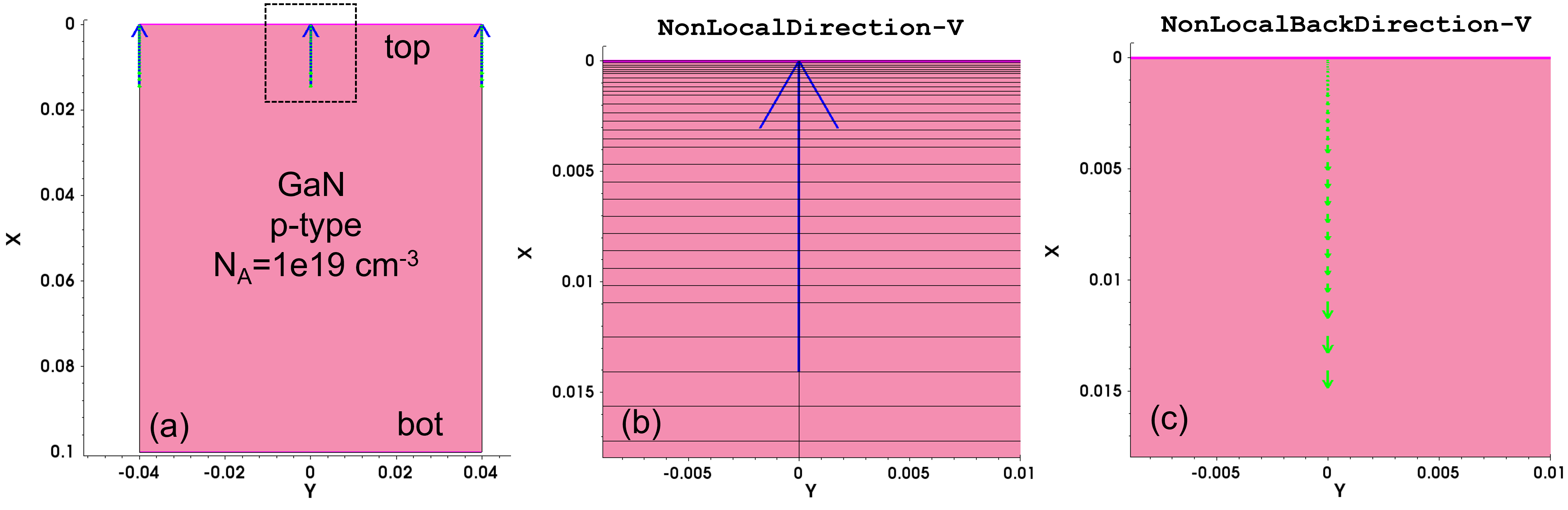
Figure 22. (Left) Schottky diode structure used in example. The top electrode is set to be of type Schottky. Nonlocal vectors (middle) and (right) correspond to the nonlocal mesh NLM_Schottky. (Click image for full-size view.)
The top electrode is defined as a Schottky contact with a gate metal Workfunction of 5.2 eV in the Electrode section of the command file:
Electrode {
   { Name= bot	Voltage= 0.0  }
   { Name= top  Voltage= 0.0  Schottky Workfunction= 5.2 }
}
Figure 23 shows the band diagrams at Vtop = 0 V and Vtop = 7 V. The band-to-band tunneling component jcv (electron tunneling from the conduction band of GaN to the metal electrode) plays a major role in contributing to the total Schottky diode current.
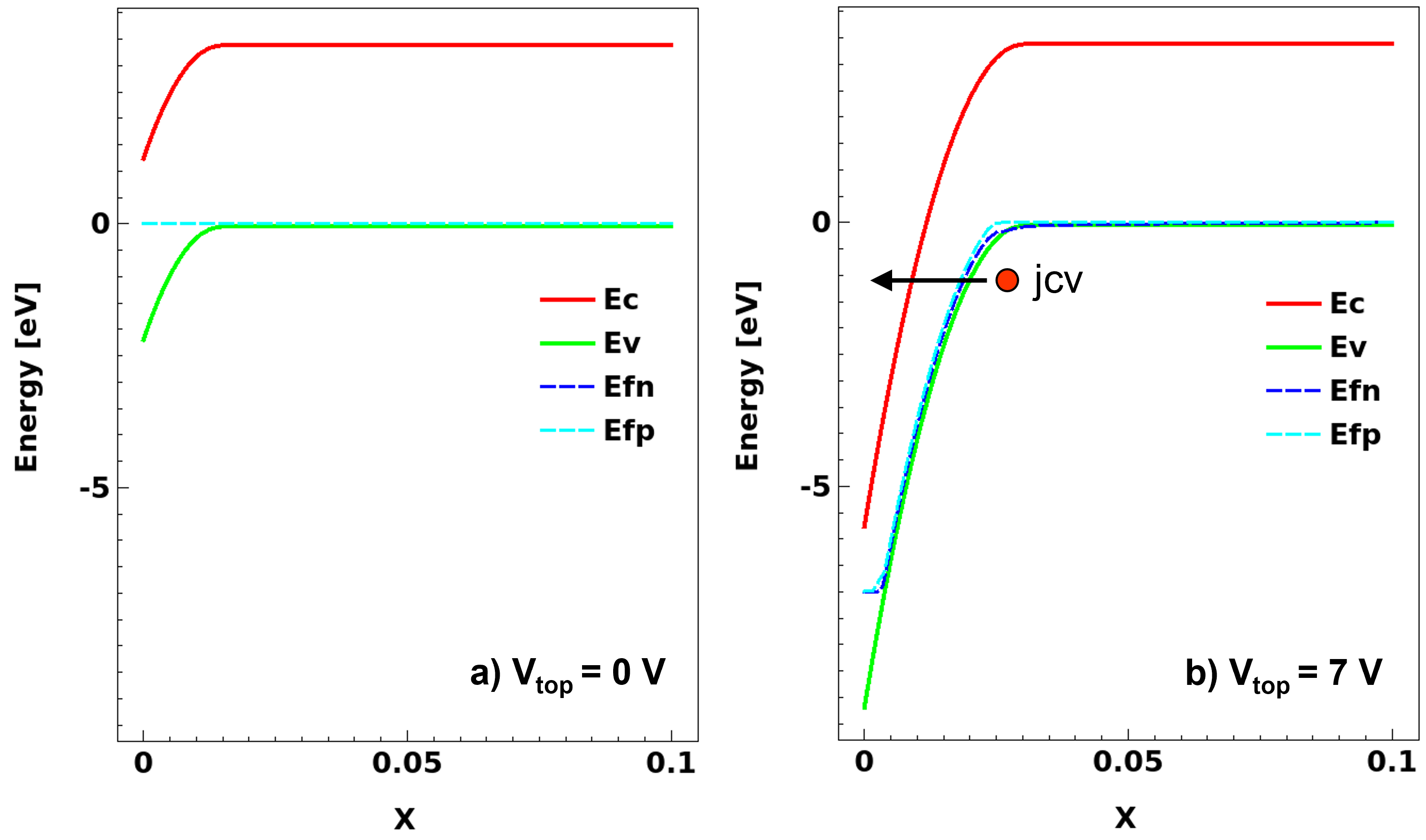
Figure 23. Band diagrams at (left) Vtop = 0 V and (right) Vtop = 7 V. Electron tunneling from conduction band of GaN to metal electrode is the dominant nonlocal tunneling component. (Click image for full-size view.)
The nonlocal tunneling model with the Band2Band option as shown here is used to account for the jcv component of the nonlocal mesh named NLM_schottky:
Physics {
   ...
   eBarrierTunneling "NLM_schottky" (Band2Band=Full)
}
The nonlocal mesh NLM_schottky is specified as shown here. The Length of the nonlocal mesh must be long enough to capture the band-edge profile in the depletion region. The Length is varied to arrive at the optimum value:
Math {
   ...
   NonLocal "NLM_schottky" (
      Electrode="top"
      Length= 12e-7
   )
}
The Length parameter is varied to study the effect of nonlocal mesh length on the Schottky diode current. Figure 24 shows that the nonlocal Length should be approximately 12 nm to accurately model the band-to-band tunneling current in the GaN Schottky diode.
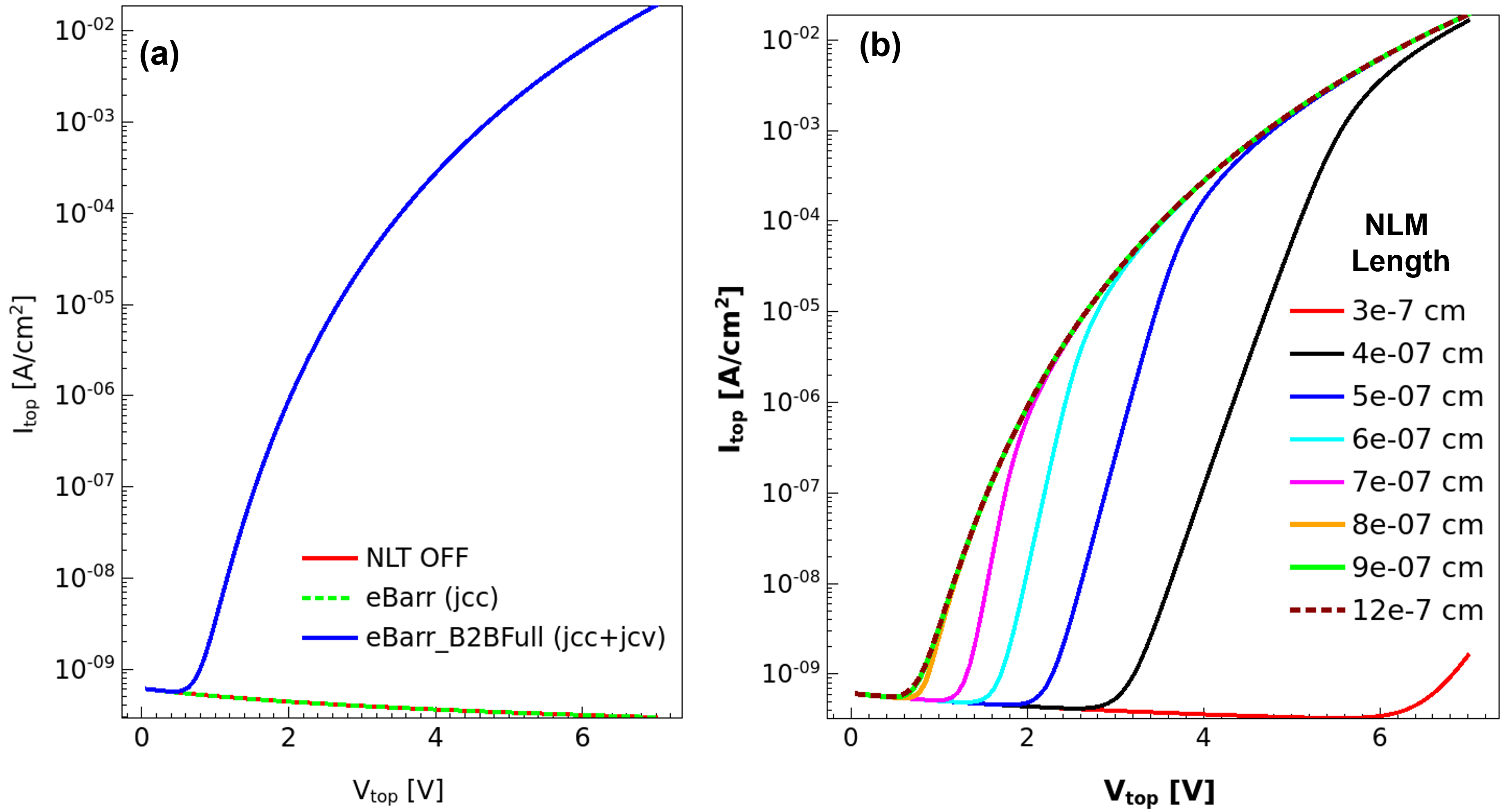
Figure 24. (Left) Schottky diode current for various simulation cases (OFF: Nonlocal tunneling OFF, eBarr: jcc, eBarr_B2BFull: jcc+jcv). (Right) Effect of nonlocal mesh length on Schottky diode current. (Click image for full-size view.)
Figure 25 shows the electron and hole tunneling generation rates for eBarr_B2BFull. Tunneling of electrons from the valence band of GaN results in the generation of holes (hBarrierTunneling) in GaN.
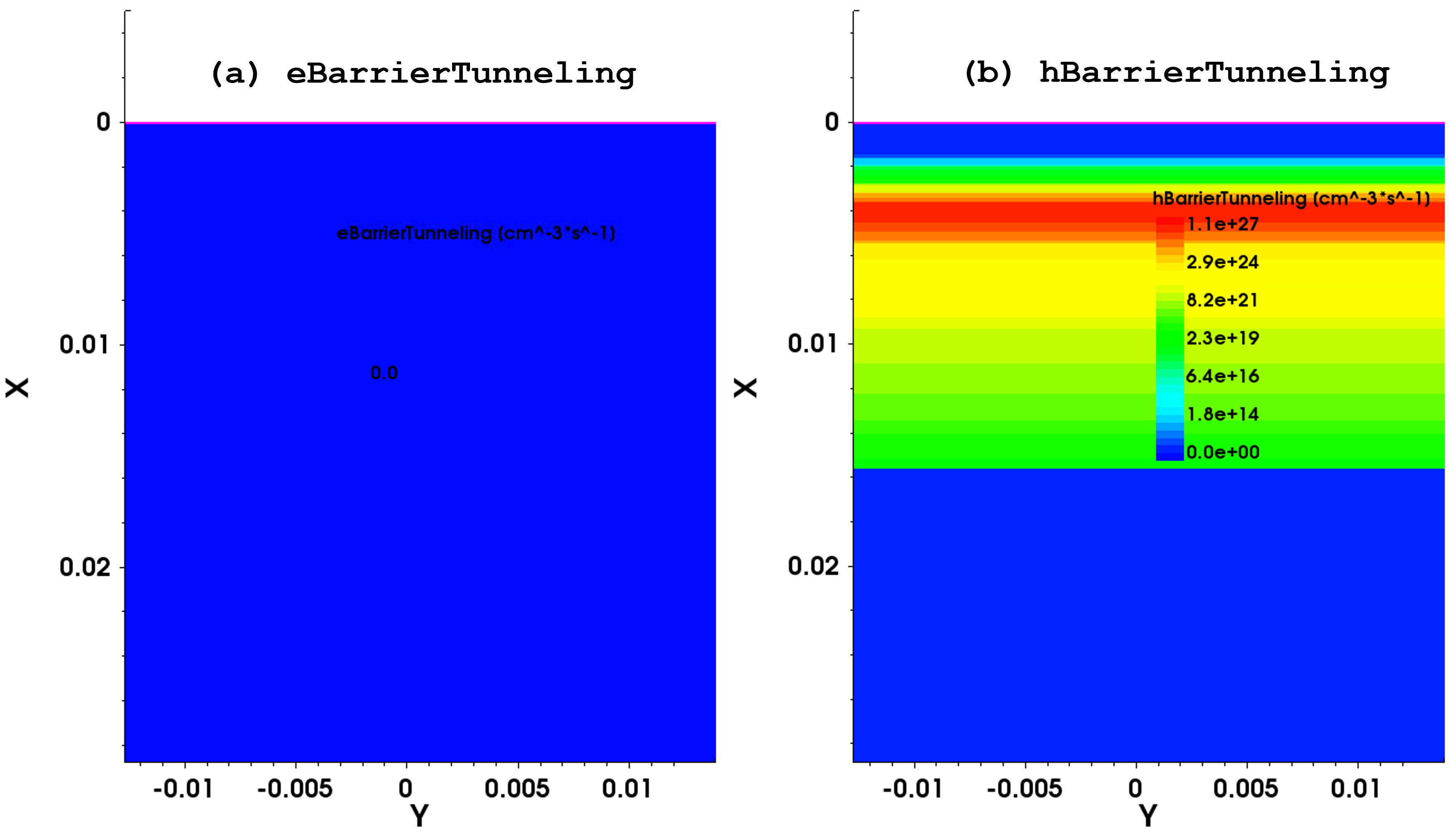
Figure 25. Carrier tunneling generation rates for eBarr_B2BFull. (Click image for full-size view.)
19.4 Example: SONOS Memory
This section discusses the setup to simulate SONOS memory.
The complete project can be investigated from within Sentaurus Workbench in the directory Applications_Library/GettingStarted/sdevice/Tunneling/SONOS_Memory.
Figure 26 (left) shows the SONOS memory structure used in this example. The magnified view of the gate stack shows the charge trap layer (CTL), tunnel oxide layer, and block oxide layer.
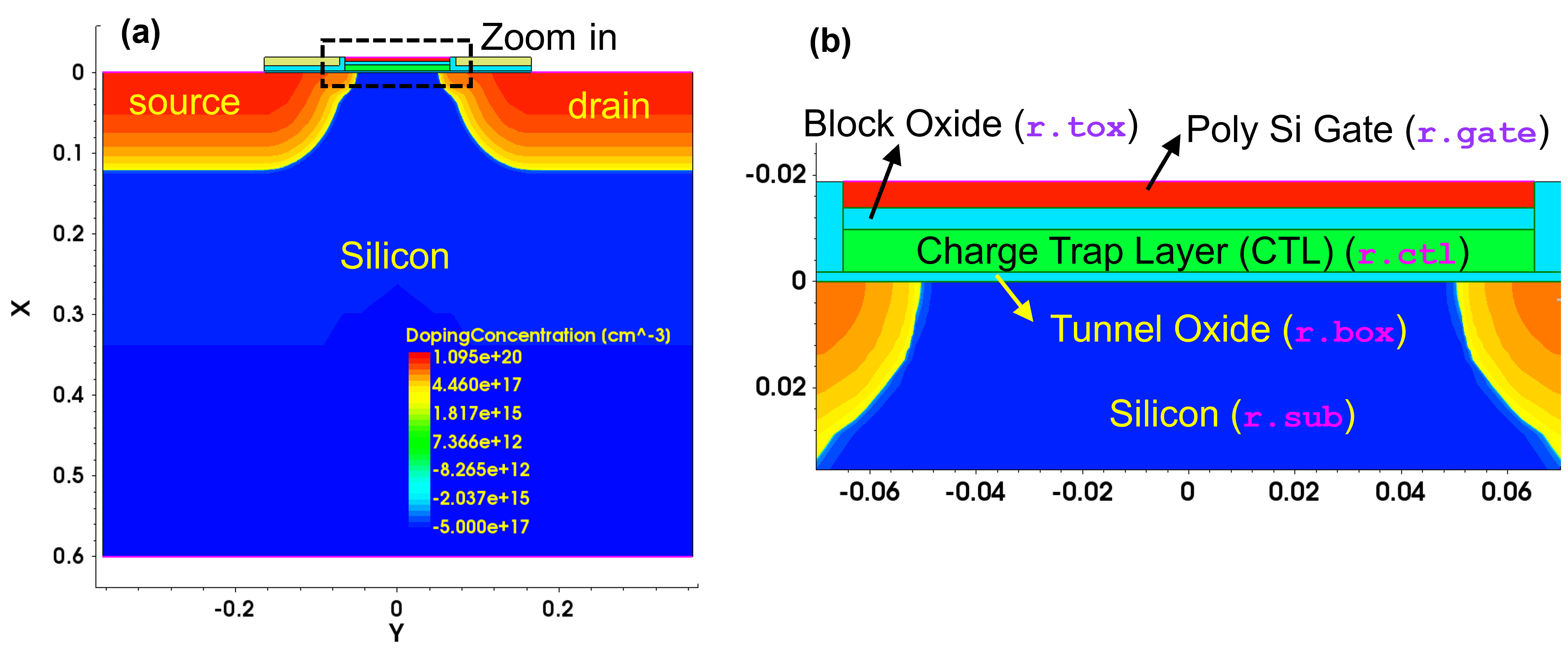
Figure 26. (Left) CTL-based memory structure used in example. (Right) Magnified view of gate stack showing CTL, tunnel oxide, and block oxide. (Click image for full-size view.)
Here, the CTL is treated as a semiconductor (NitrideAsSemiconductor), which allows for the modeling of the relevant physics within this critical layer. Figure 27 illustrates various relevant mechanisms during programming. For simplicity, the electron picture is used here for illustration:
- Capture and emission of carriers from and to the conduction band or valence band (process 1)
- Tunneling of carriers directly into or out of the traps in the CTL (processes 2 and 3)
- Tunneling of carriers into or out of the conduction band or valence band (process 4)
- Redistribution of carriers due to drift-diffusion (process 5)
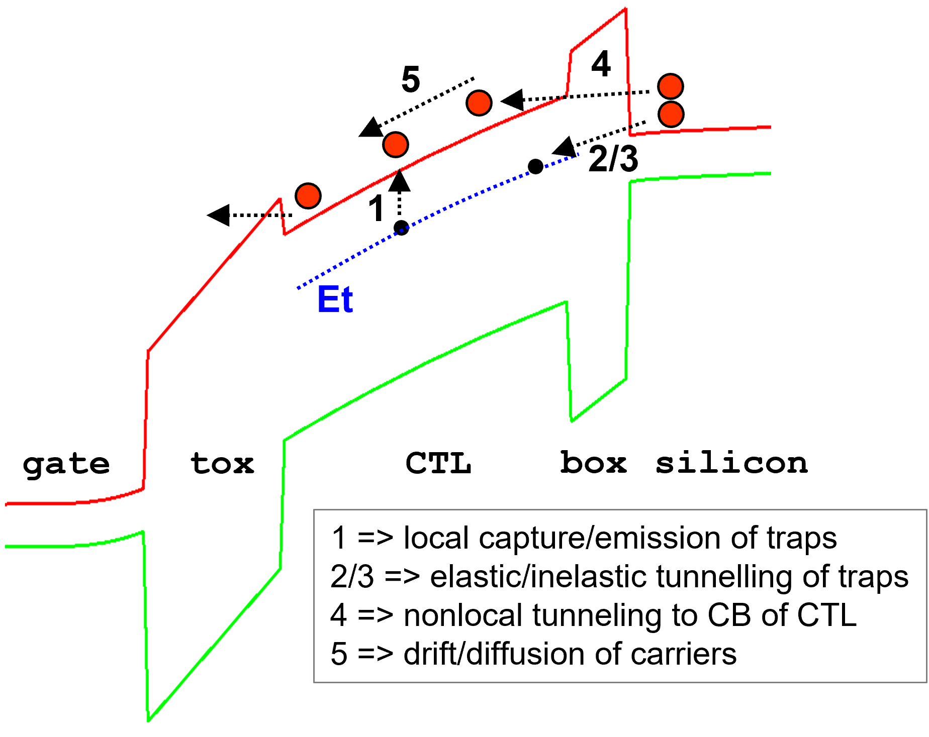
Figure 27. Various physical mechanisms in SONOS memory. (Click image for full-size view.)
SONOS memory is based on tunneling of carriers from and to the CTL, that is, the CTL is coupled to both the substrate and gate regions through tunneling. To facilitate this, two nonlocal meshes are required. Figure 28 shows the nonlocal mesh specifications (NLM_box and NLM_tox) and the resulting nonlocal vectors and nonlocal mesh (band diagrams along the nonlocal mesh). The nonlocal mesh lines of NLM_box start at the r.box/r.sub interface and end in the CTL, thereby coupling the substrate with the CTL. Similarly, the nonlocal mesh lines of NLM_tox start at the r.tox/r.gate interface and end in the CTL, thereby coupling the gate with the CTL.
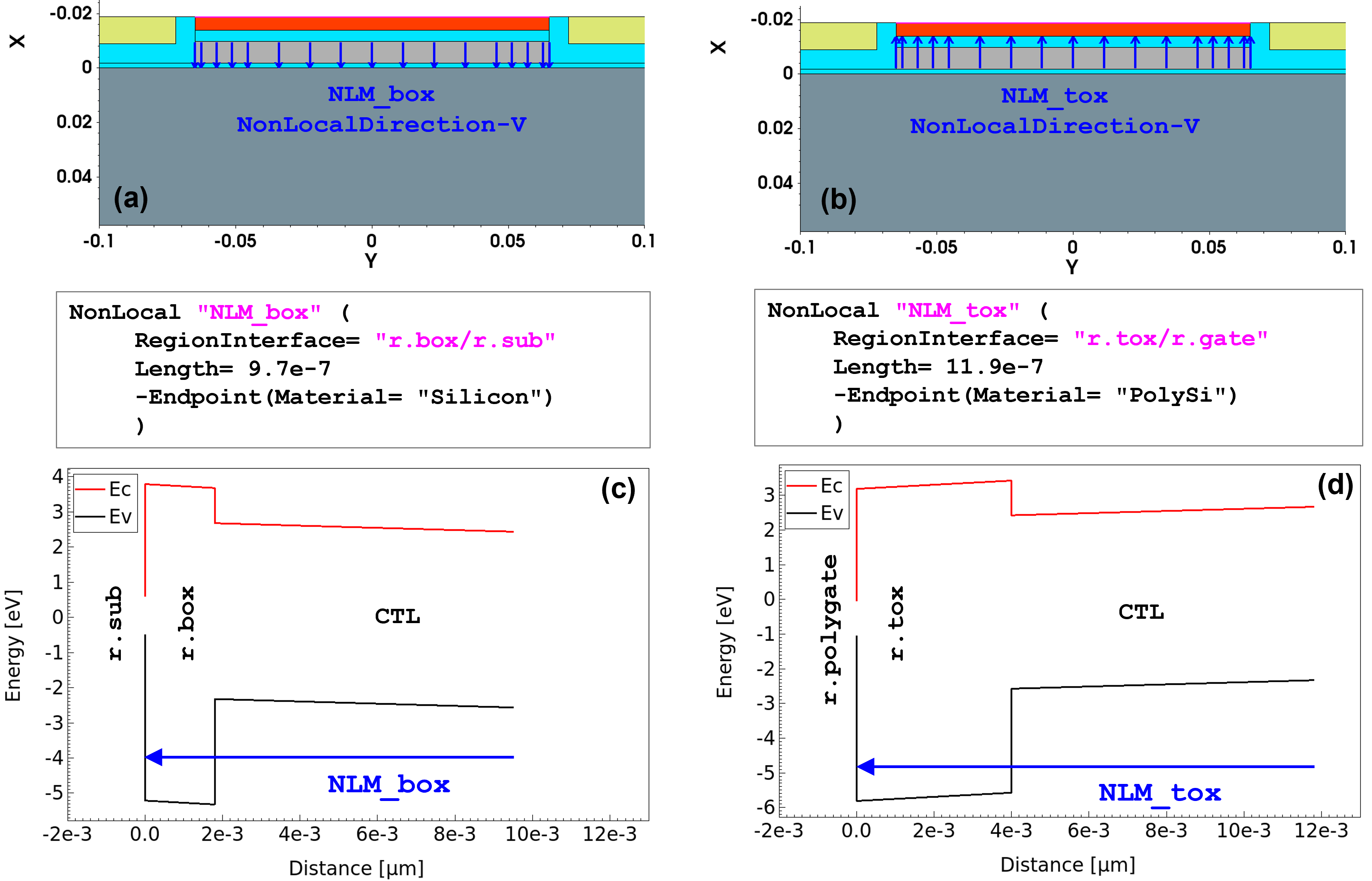
Figure 28. Nonlocal mesh specifications and corresponding nonlocal mesh vectors (a), (b), and nonlocal mesh plots (c), (d). (Click image for full-size view.)
Tunneling into and out of the CTL occurs by activating e|hBarrierTunneling for the nonlocal meshes NLM_box and NLM_tox:
Physics {
   eBarrierTunneling "NLM_box"
   hBarrierTunneling "NLM_box"
   eBarrierTunneling "NLM_tox"
   hBarrierTunneling "NLM_tox"
}
The inclusion of e|hBarrierTunneling in the Traps statement allows for the tunneling of electrons or holes directly into and out of the traps. Tunneling is activated for the nonlocal meshes NLM_box and NLM_tox. These named nonlocal meshes connect the trap locations inside the NitrideAsSemiconductor region with the interfaces of the oxide layers – r.box/r.sub and r.tox/r.gate:
Physics(Region="r.ctl") {
   Traps(
	(Donor Level EnergyMid= 3 FromConductionBand
	 Conc= 1e19
	 eXSection= 1e-15 hXSection= 1e-15
	 eBarrierTunneling(NonLocal= "NLM_tox" NonLocal= "NLM_box")
	 hBarrierTunneling(NonLocal= "NLM_tox" NonLocal= "NLM_box")
	 TrapVolume= 1e-15
	)

	(Acceptor Level EnergyMid= 2 FromValenceBand
	 Conc= 1e19
	 eXSection= 1e-15 hXSection= 1e-15
	 eBarrierTunneling(NonLocal= "NLM_tox" NonLocal= "NLM_box")
	 hBarrierTunneling(NonLocal= "NLM_tox" NonLocal= "NLM_box")
	 TrapVolume= 1e-15
	)
   )
}
Figure 29 shows the tunneling generation rates for program and erase biasing conditions. For program conditions, you use gate biasing of Vg= 9 V (see Figure 29 (left)). The generation rate, shown on the Y1 axis is -ve at the channel–tunnel-oxide interface. This shows that electrons tunnel out from the channel and tunnel into the traps in the CTL (see the positive generation in the middle of the CTL). You can also see that some electrons tunnel out from the CTL into the gate – this is unwanted back-tunneling that designers try to reduce.
Figure 30 (left) further confirms this tunneling into the CTL since you can see that the concentration of electrons (eDensity field) in the CTL increases by several orders of magnitude compared to equilibrium (Vg= 0 V).
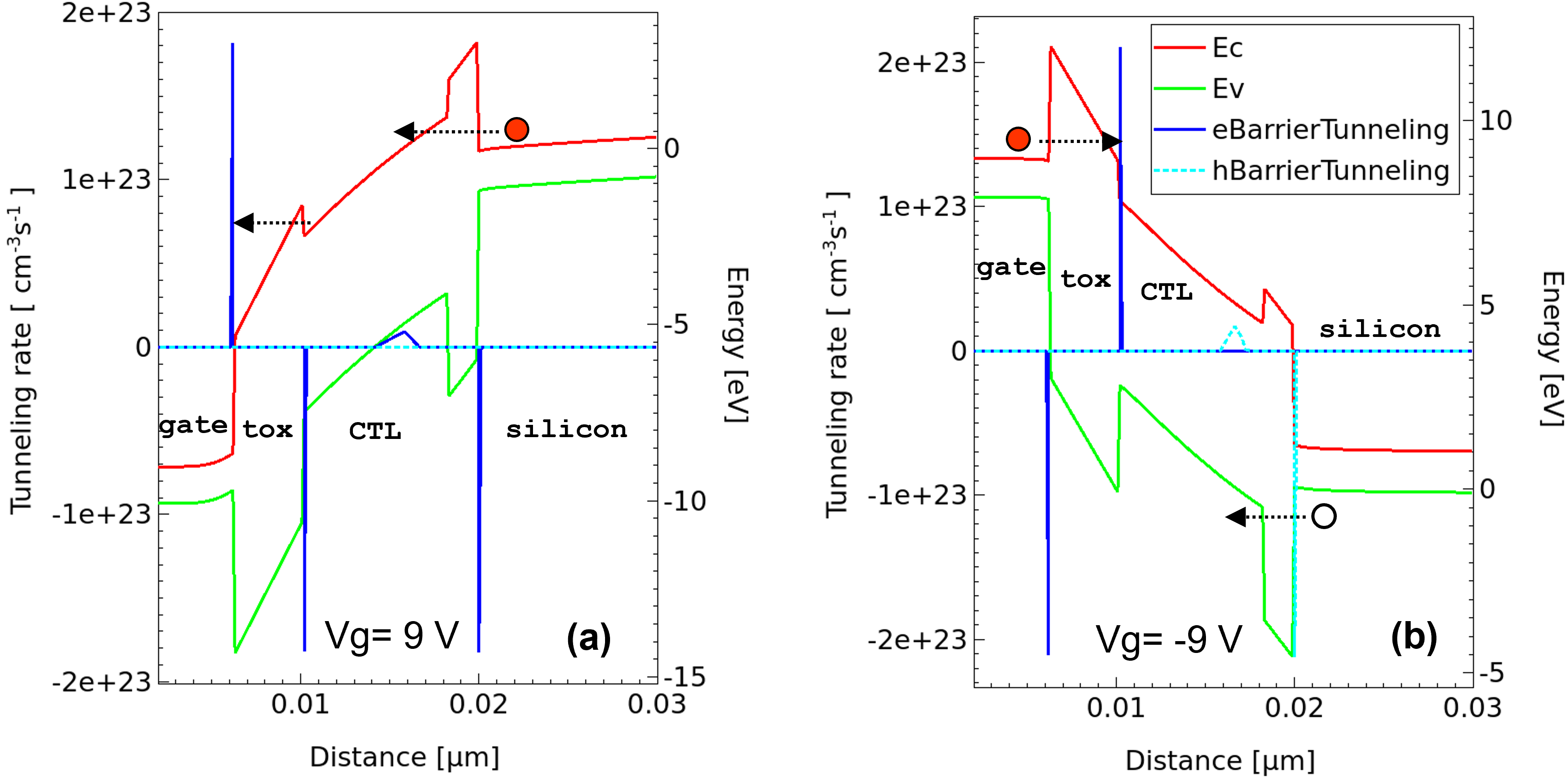
Figure 29. Tunneling generation rates for program (Vg= 9 V) and erase (Vg= -9 V) biasing conditions. (Click image for full-size view.)
For erase gate biasing of Vg= -9 V (Figure 29 (right), the hBarrierTunneling rates indicate tunneling of holes from the channel to the CTL, and the eBarrierTunneling rates indicate tunneling of electrons from the gate to the CTL. This is reflected as an increase in hDensity and eDensity (see Figure 30 (right)) by several orders of magnitude compared to equilibrium (Vg= 0 V).
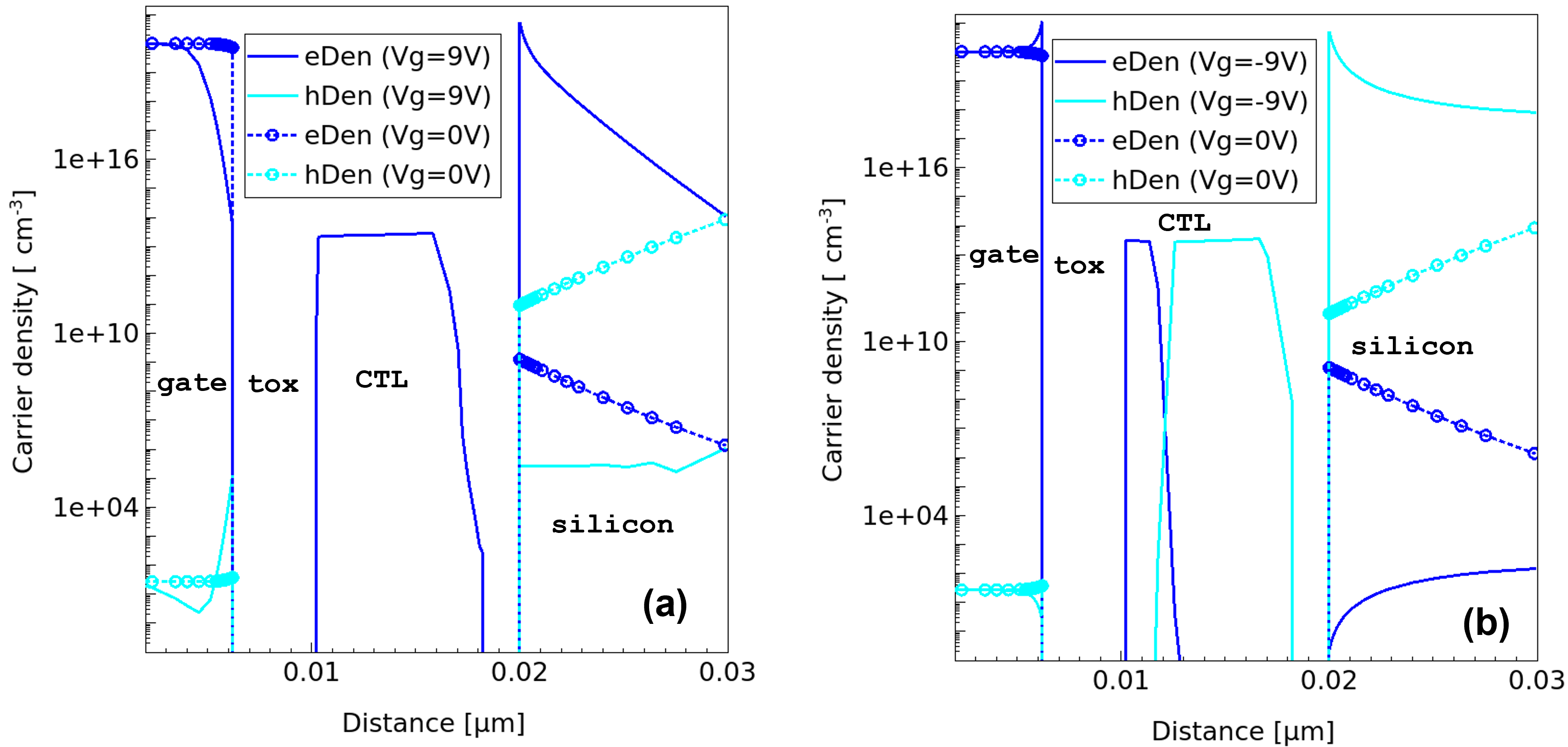
Figure 30. Carrier density for program (Vg= 9 V) and erase (Vg= -9 V) biasing conditions. (Click image for full-size view.)
Figure 31 shows the trapped carrier density for program and erase biasing conditions. Such trapped carrier density results from two tunneling events occurring simultaneously. One is due to carriers tunneling (from the substrate or gate) to the conduction band of the CTL. The other is due to carriers tunneling (from the substrate or gate) directly to the trap locations (trap energy level) in the CTL.
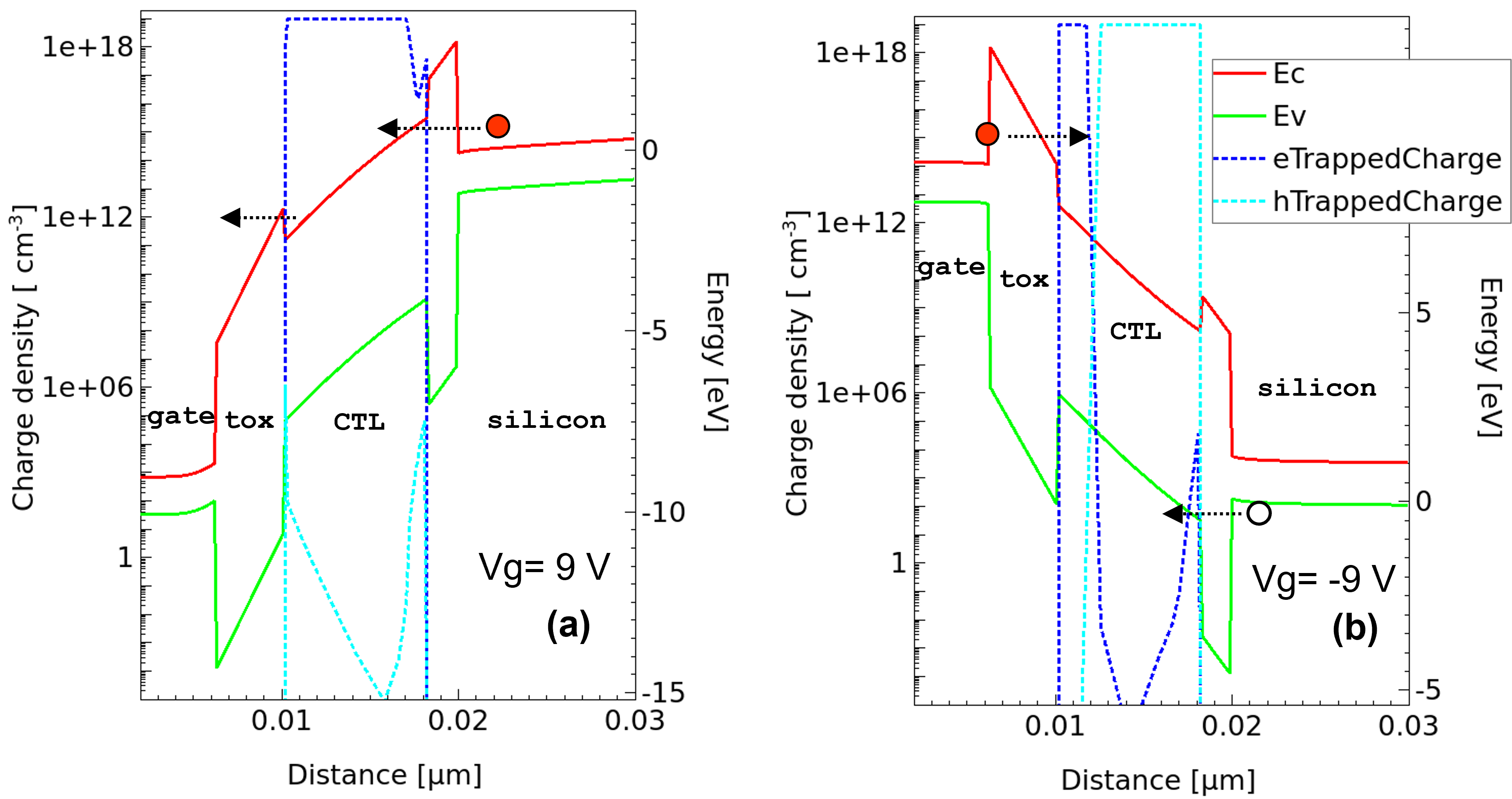
Figure 31. Trapped carrier density for program (Vg= 9 V) and erase (Vg= -9 V) biasing conditions. (Click image for full-size view.)
19.5 Example: Tunnel Diode
Tunnel pn diodes operate based on band-to-band tunneling between heavily doped p- and n-regions. The two main groups of band-to-band tunneling models implemented in Sentaurus Device are nonlocal tunneling models and local tunneling models.
The nonlocal band-to-band tunneling models compute the tunneling generation–recombination rate by integrating over the tunneling path. In contrast, the local tunneling models compute this rate at a point from the electric field value or the gradient of the Fermi potential at that point. The nonlocal models take into account the energy band profile as well as the spatial transport of carriers; whereas, for local tunneling models, there is no carrier transport. Accurate modeling of the I–V characteristics of the tunnel diode requires a nonlocal band-to-band tunneling model.
Band-to-band tunneling in a tunnel diode can be implemented using the nonlocal tunneling model (with the Band2Band option and an appropriate nonlocal mesh specification). Sentaurus Device provides yet another nonlocal band-to-band tunneling model that can be used for tunnel diode simulations – the dynamic nonlocal path band-to-band tunneling model. It would be useful to recall the two nonlocal band-to-band tunneling models implemented in Sentaurus Device:
- Predefined nonlocal mesh–based nonlocal tunneling model (static)
- Dynamic nonlocal path band-to-band tunneling model (dynamic)
This section examines a GaAs tunnel diode simulation using both these approaches. Figure 32 (left) shows the tunnel diode structure used in this example (TunnelDiode), and Figure 32 (right) shows the equilibrium band diagram typical for a pn junction diode. The band-to-band tunneling components (Jcv and Jvc) that are critical for tunnel diode operation are noted.
The complete project can be investigated from within Sentaurus Workbench in the directory Applications_Library/GettingStarted/sdevice/Tunneling/TunnelDiode.
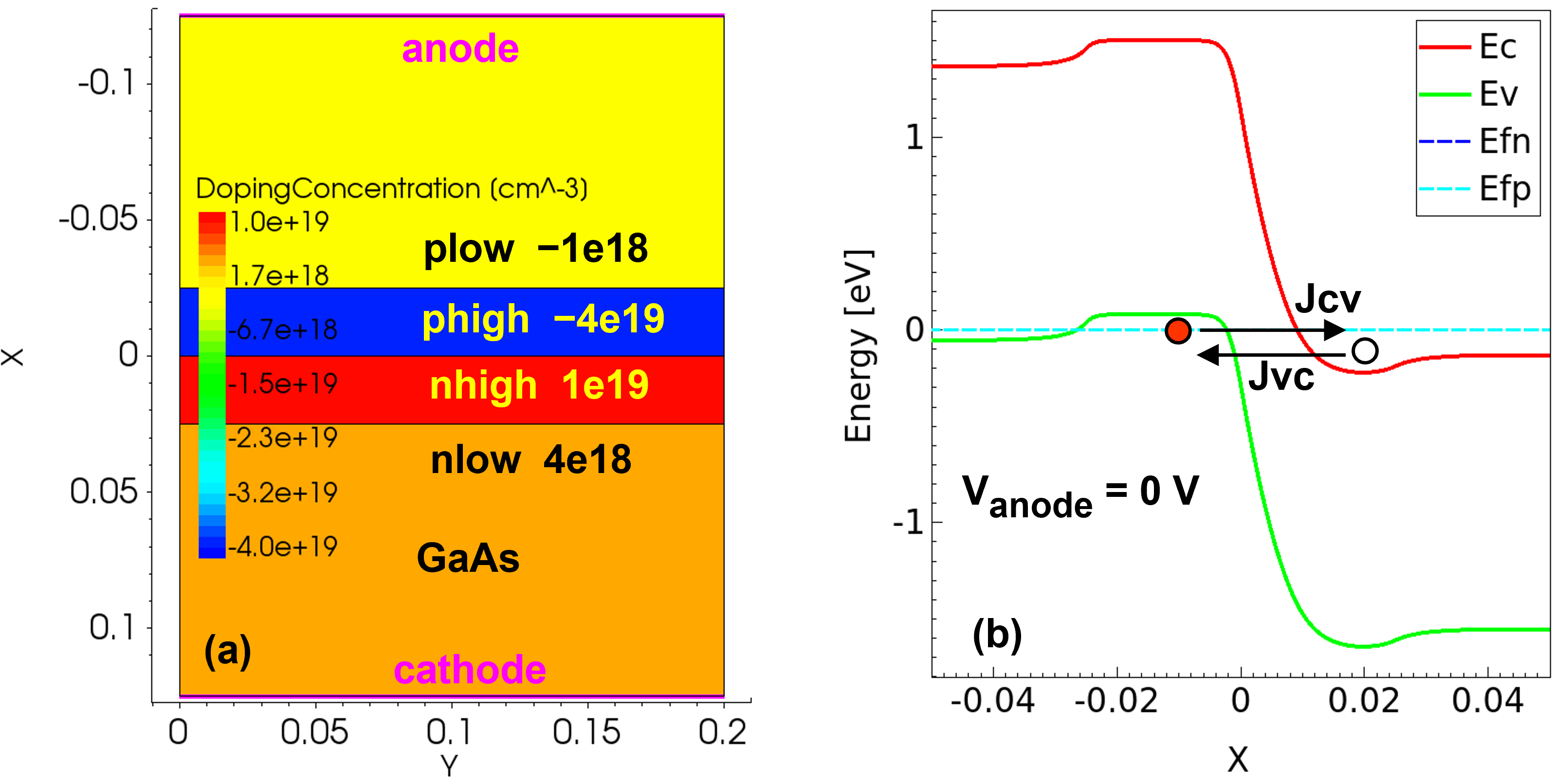
Figure 32. (Left) Tunnel diode structure and (right) equilibrium band diagram, noting the band-to-band tunneling components Jcv and Jvc. (Click image for full-size view.)
This section covers the following topics:
- Section 19.5.1 Using Nonlocal Tunneling Model
- Section 19.5.2 Using Dynamic Nonlocal Path Band-to-Band Tunneling Model
19.5.1 Using Nonlocal Tunneling Model
The nonlocal mesh should be long enough to capture the band-edge profile that is required for band-to-band tunneling as shown in Figure 32 (right). However, the nonlocality of tunneling can increase the simulation time dramatically. To optimize the simulation time, the following nonlocal mesh specification is used. To limit the speed degradation, Length and Permeation should be as small as possible. The nonlocal parameter Length is set to 40e-7 and Permeation is varied to study the extent of the band-edge profile covered:
Nonlocal "NLM" (
   RegionInterface="phigh/nhigh"
   Length=40e-7
   Permeation = _Permeation_
)
Figure 33 shows the effect of Permeation on the nonlocal mesh and band-edge profile coverage. As can be seen when Permeation=0, neither of the nonlocal lines NLMn or NLMp covers the band-edge profile required for tunneling. By increasing Permeation, the total length of the nonlocal lines increases, thereby covering the relevant band-edge profile.
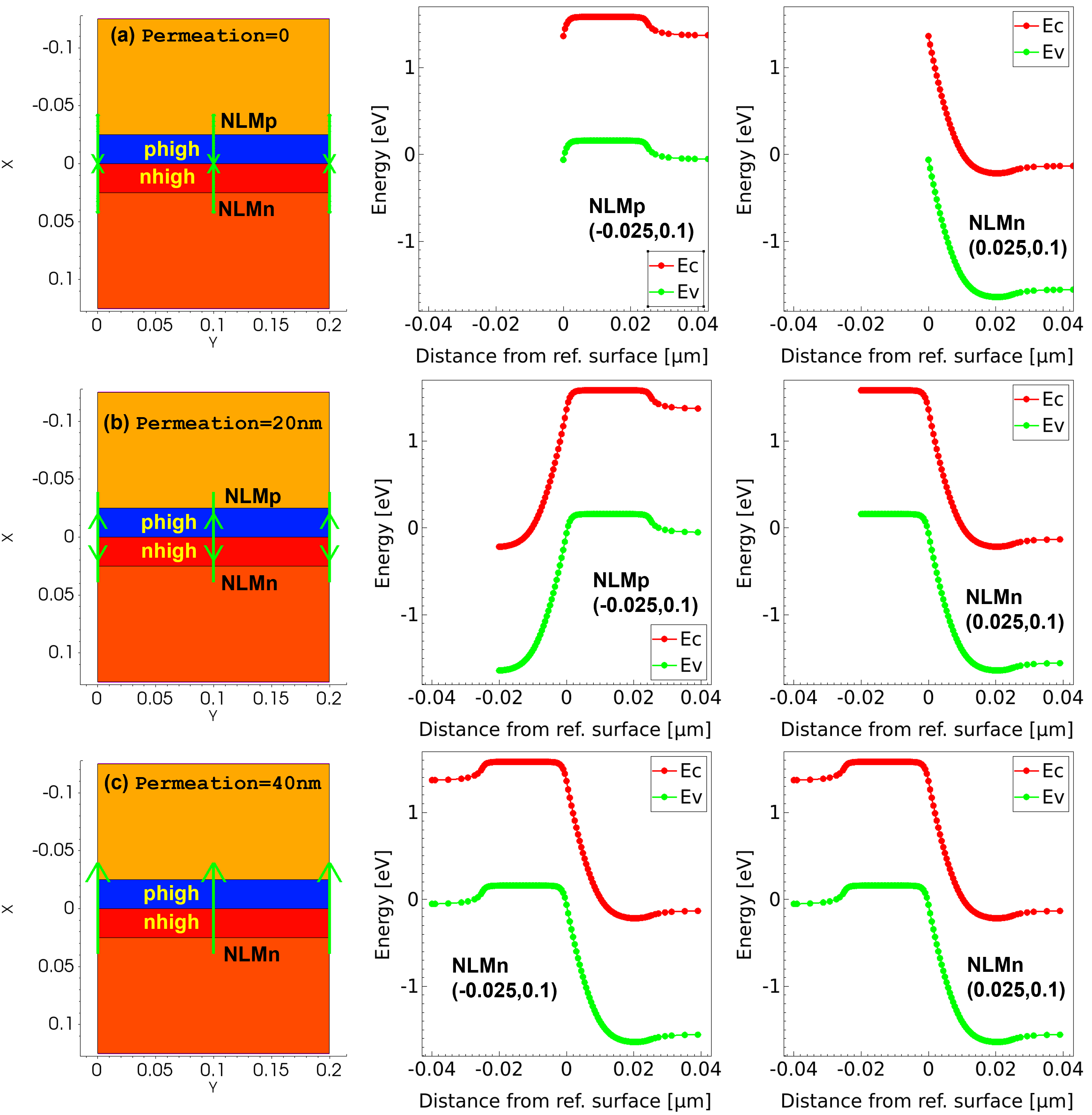
Figure 33. Effect of Permeation on nonlocal mesh. (Click image for full-size view.)
Figure 34 shows the effect of Permeation on the tunneling current. As can be seen when Permeation=0, the pn diode shows reverse saturation current, typical of a conventional pn diode. In Figure 33 and Figure 34, you can see that a Permeation of approximately 20 nm would be required in this case to accurately model the tunnel diode.
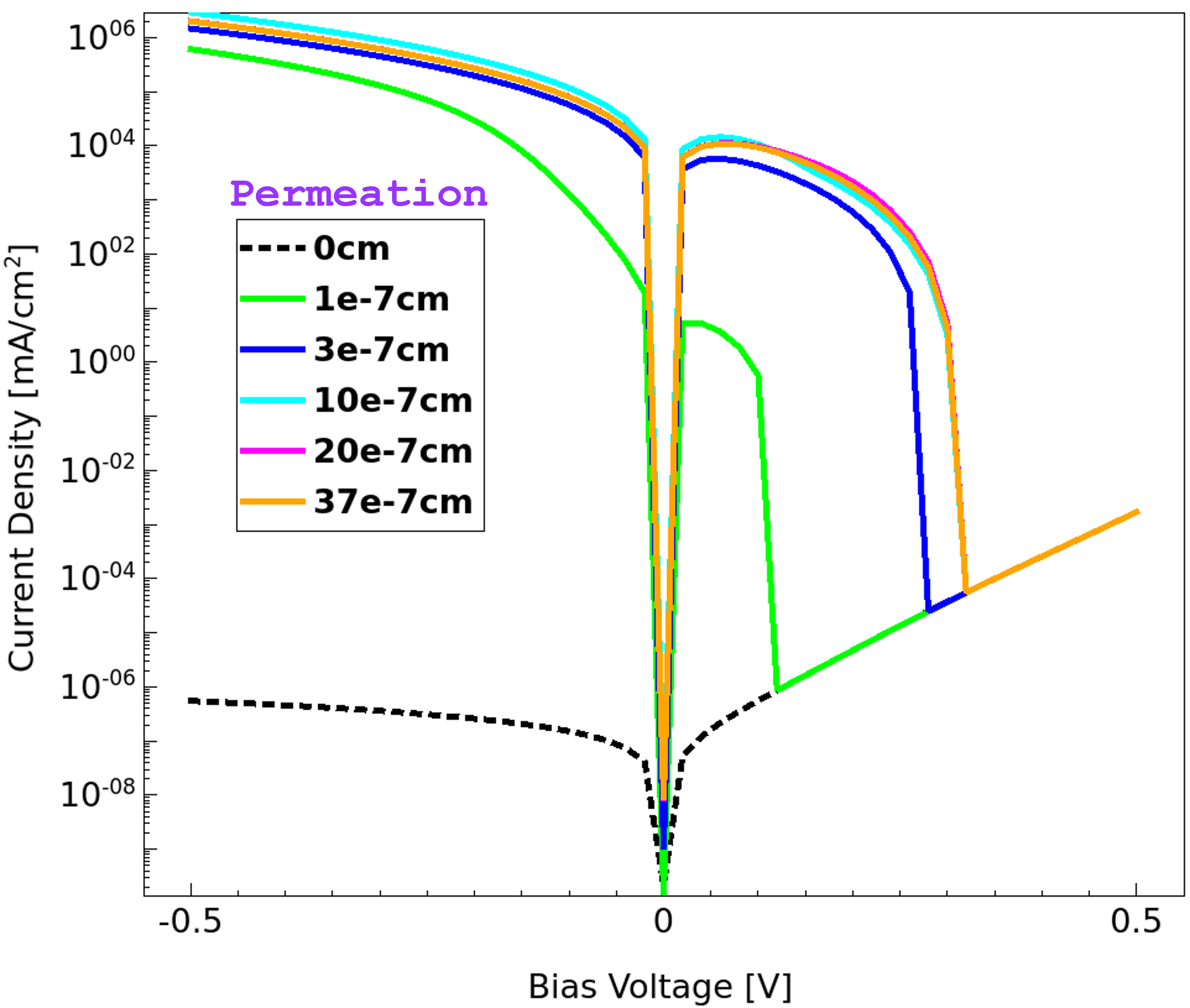
Figure 34. Effect of Permeation on nonlocal tunneling current. (Click image for full-size view.)
19.5.2 Using Dynamic Nonlocal Path Band-to-Band Tunneling Model
When the dynamic nonlocal path band-to-band tunneling model is used, the tunneling path is determined dynamically based on the energy band profile. Therefore, this model does not require user-specification of the nonlocal mesh. This is in contrast to the nonlocal tunneling model, which is based on a predefined and static nonlocal mesh.
The dynamic nonlocal path band-to-band tunneling model computes the band-to-band tunneling generation rate using a WKB path-integral formulation. The following expressions summarize the model in reduced form (the well-known Kane and Keldysh models) in the uniform electric-field limit, noting the parameters that can be modified in the parameter file.
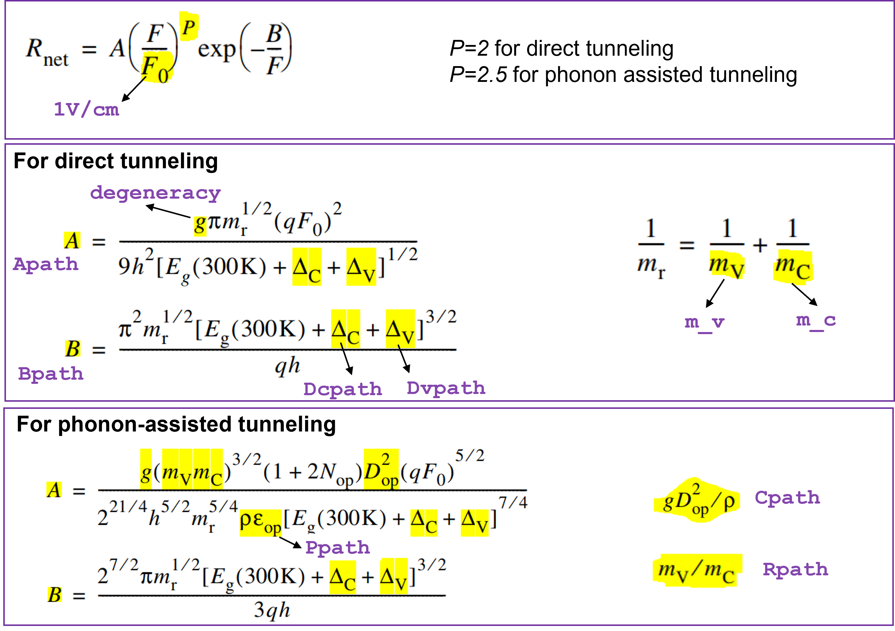
The dynamic nonlocal path band-to-band tunneling model is activated using the keyword NonlocalPath in the Band2Band option of Recombination in the Physics section:
Physics {
   ...
   Recombination (
      ...
      Band2Band(Model=NonlocalPath)
   )
}
The parameter values of the dynamic nonlocal path band-to-band tunneling model are specified in the Band2BandTunneling parameter set. In direct semiconductors such as GaAs, the direct tunneling process is dominant. The tunneling process is specified as direct by setting the phonon energy parameter Ppath equal to zero in the parameter set. The maximum length of the tunneling path, MaxTunnelLength, is used to limit the tunneling path length to the specified value:
Band2BandTunneling
{
   Apath	= 1e19		# [1/cm^3/s]
   Bpath	= 1.05e7	# [V/cm]
   Dcpath	= 0.0000e+00	# [eV]
   Dvpath	= 0.0000e+00	# [eV]
   Ppath	= 0.0000e+00	# [eV]
   Rpath	= 0.0000e+00	# [1]
   MaxTunnelLength = 1.0000e-05	# [cm]
}
The GaAs tunnel diode I–V characteristics can be fine-tuned using the parameters Apath and Bpath. Figure 35 shows the effect of varying the Apath and Bpath parameters on the tunnel diode current.
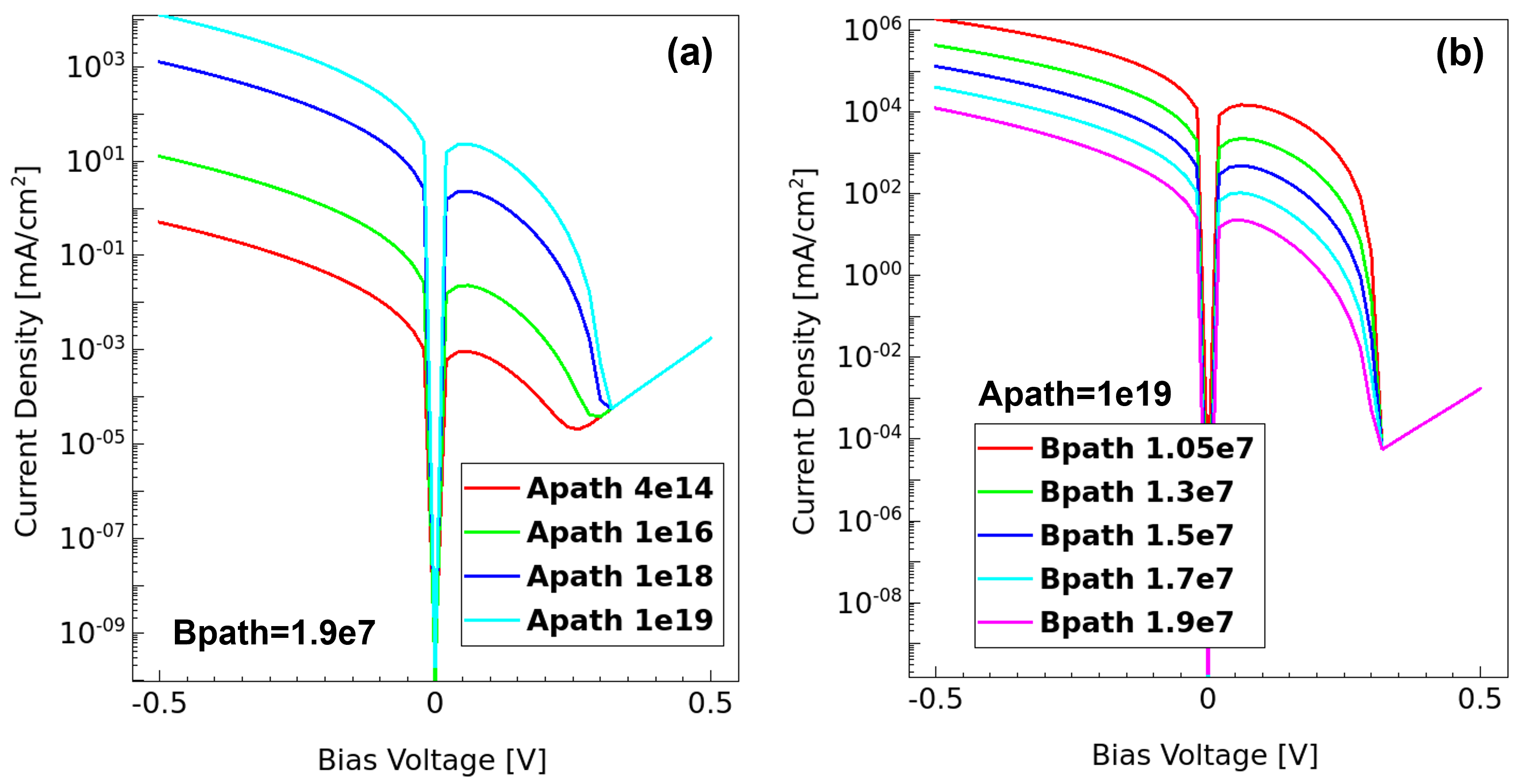
Figure 35. Effect of parameters Apath and Bpath on tunnel diode current. (Click image for full-size view.)
Figure 36 shows that, by fine-tuning the model parameters, both nonlocal band-to-band tunneling models (static and dynamic) give similar band-to-band tunneling currents.
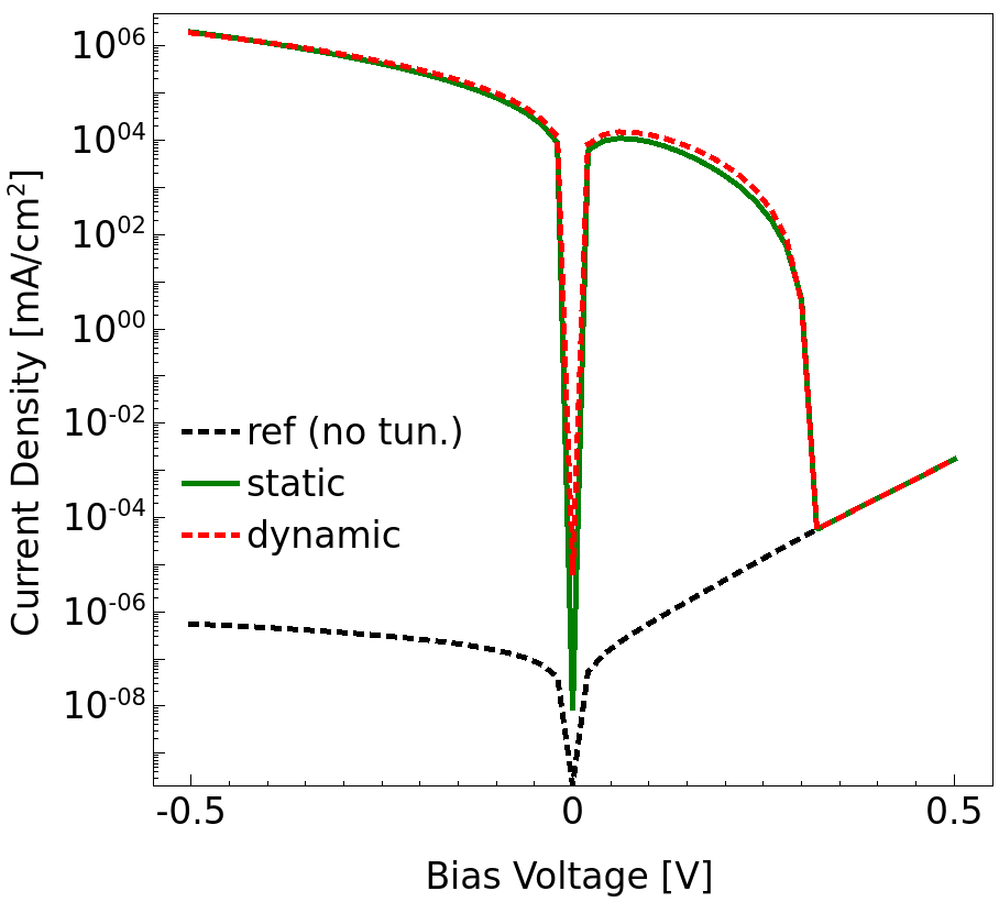
Figure 36. Dynamic nonlocal path versus static nonlocal mesh–based band-to-band tunneling. (Click image for full-size view.)
To plot the electron and hole generation rates, specify eBand2BandGeneration and hBand2BandGeneration in the Plot section, respectively. Band2BandGeneration is the same as hBand2BandGeneration. For example:
Plot {
   ...
   eBand2BandGeneration hBand2BandGeneration Band2BandGeneration
}
The band-to-band tunneling generation rate is positive under reverse bias (since carriers are generated) and negative under forward bias (since carriers are lost).
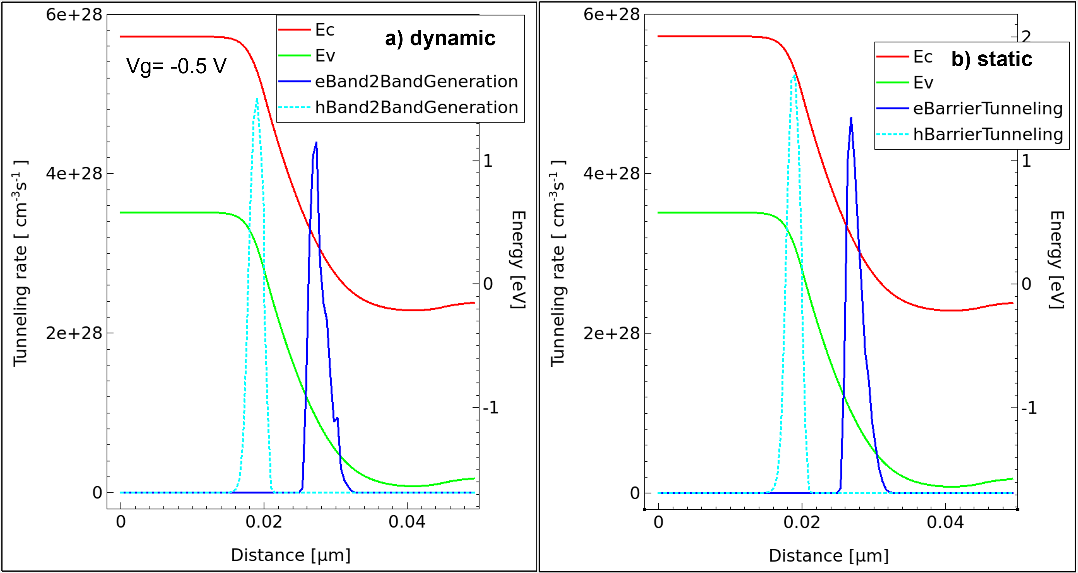
Figure 37. Tunneling generation rates for (left) dynamic model and (right) static model. (Click image for full-size view.)
19.6 Assignment
This section presents the following example projects:
19.6.1 Example: MOSFET GIDL
Gate-induced drain leakage (GIDL) is due to band-to-band tunneling in silicon near the gate–drain overlap region. GIDL is pronounced at high drain bias and low gate bias conditions. Under such bias conditions, electrons tunnel from the valence band of the substrate region into the conduction band of the drain region.
The project (MOSFET_GIDL) includes structure generation and Id–Vg simulation. You are encouraged to modify the Sentaurus Device command file to account for GIDL.
The complete project can be investigated from within Sentaurus Workbench in the directory Applications_Library/GettingStarted/sdevice/Tunneling/MOSFET_GIDL.
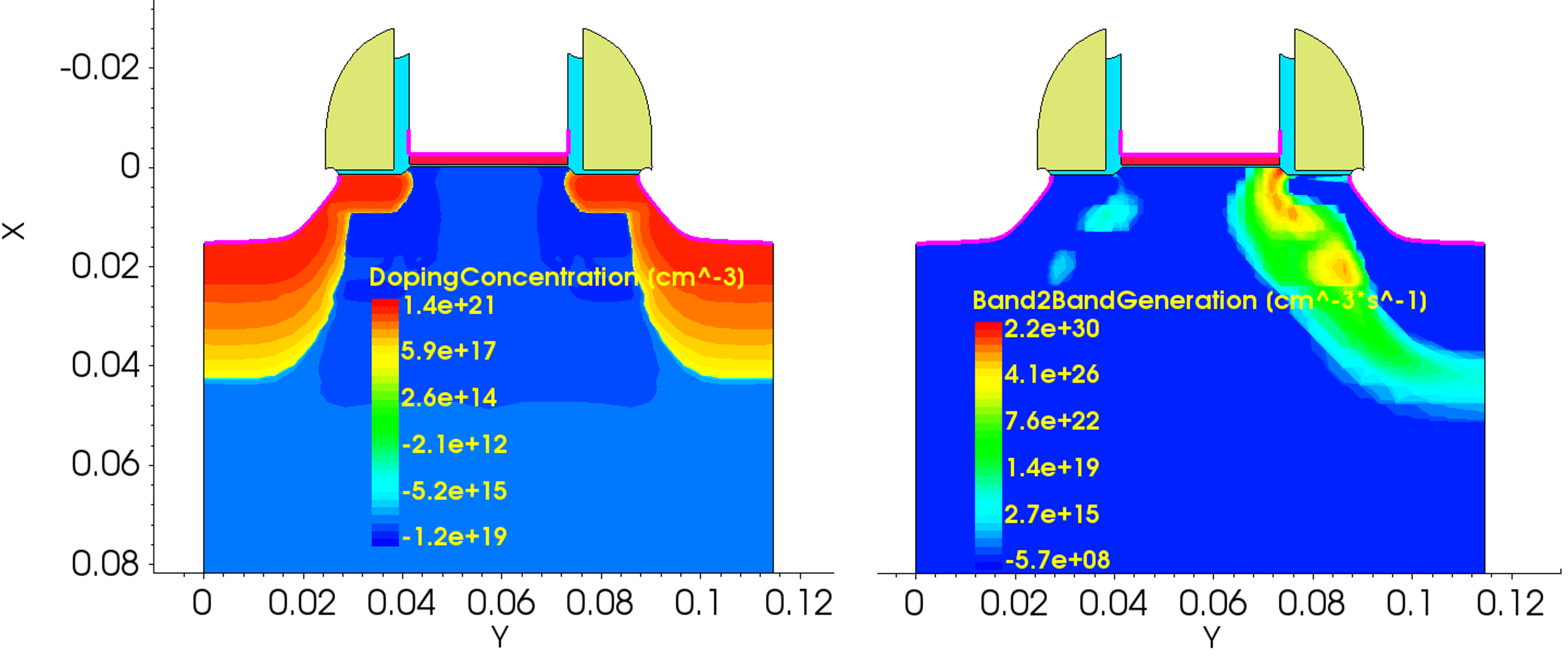
Figure 38. Simulation of GIDL in MOSFET. (Click image for full-size view.)
19.6.2 Example: Tunnel FET
Figure 39 shows a basic tunnel FET structure, which is based on band-to-band tunneling. Figure 40 shows the band diagrams (at Vds=1) for Vg=0 V and Vg= 3 V. As can be seen at Vg= 3 V, the tunneling distance reduces and the band-to-band tunneling model must be included.
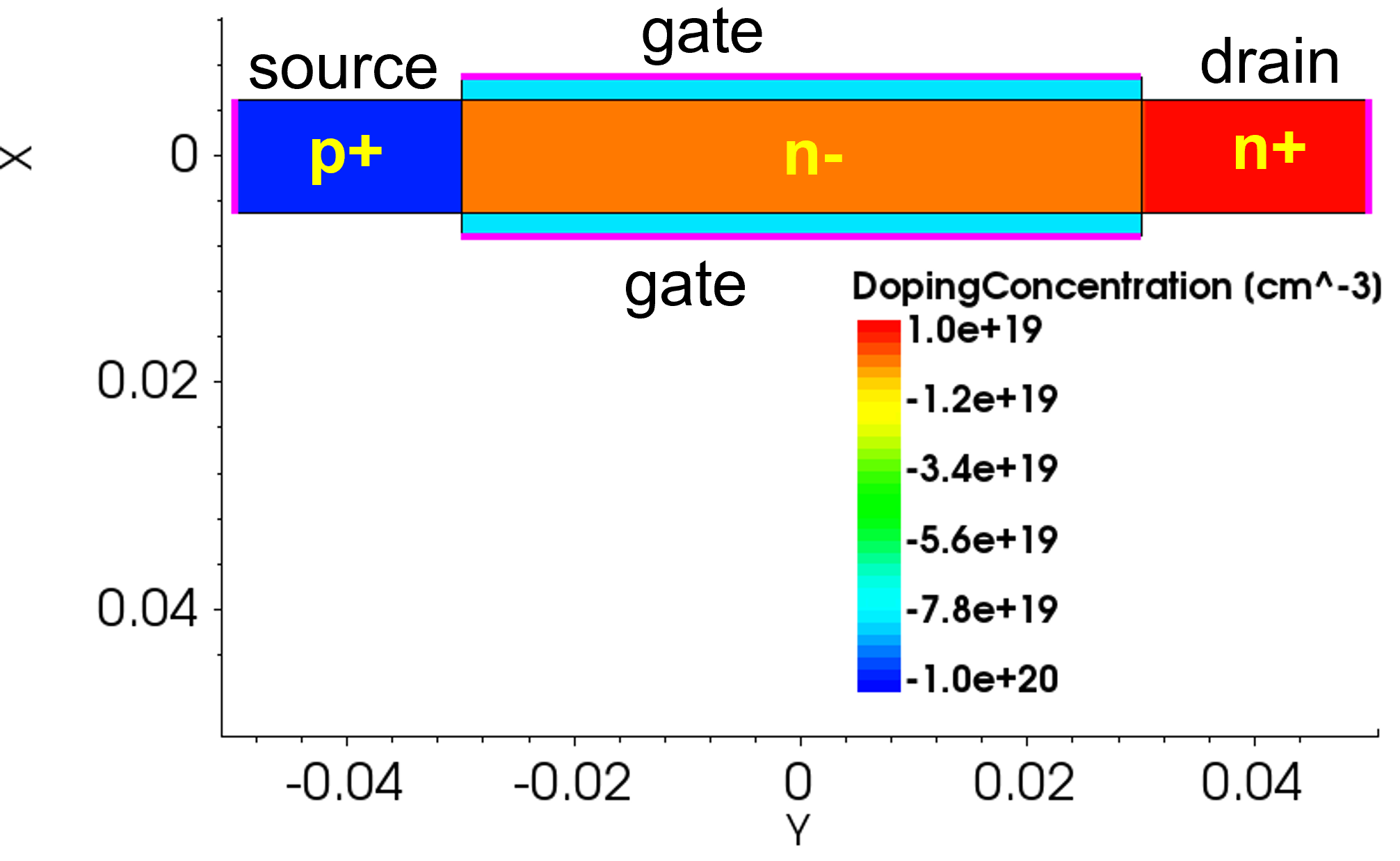
Figure 39. Structure of tunnel FET. (Click image for full-size view.)
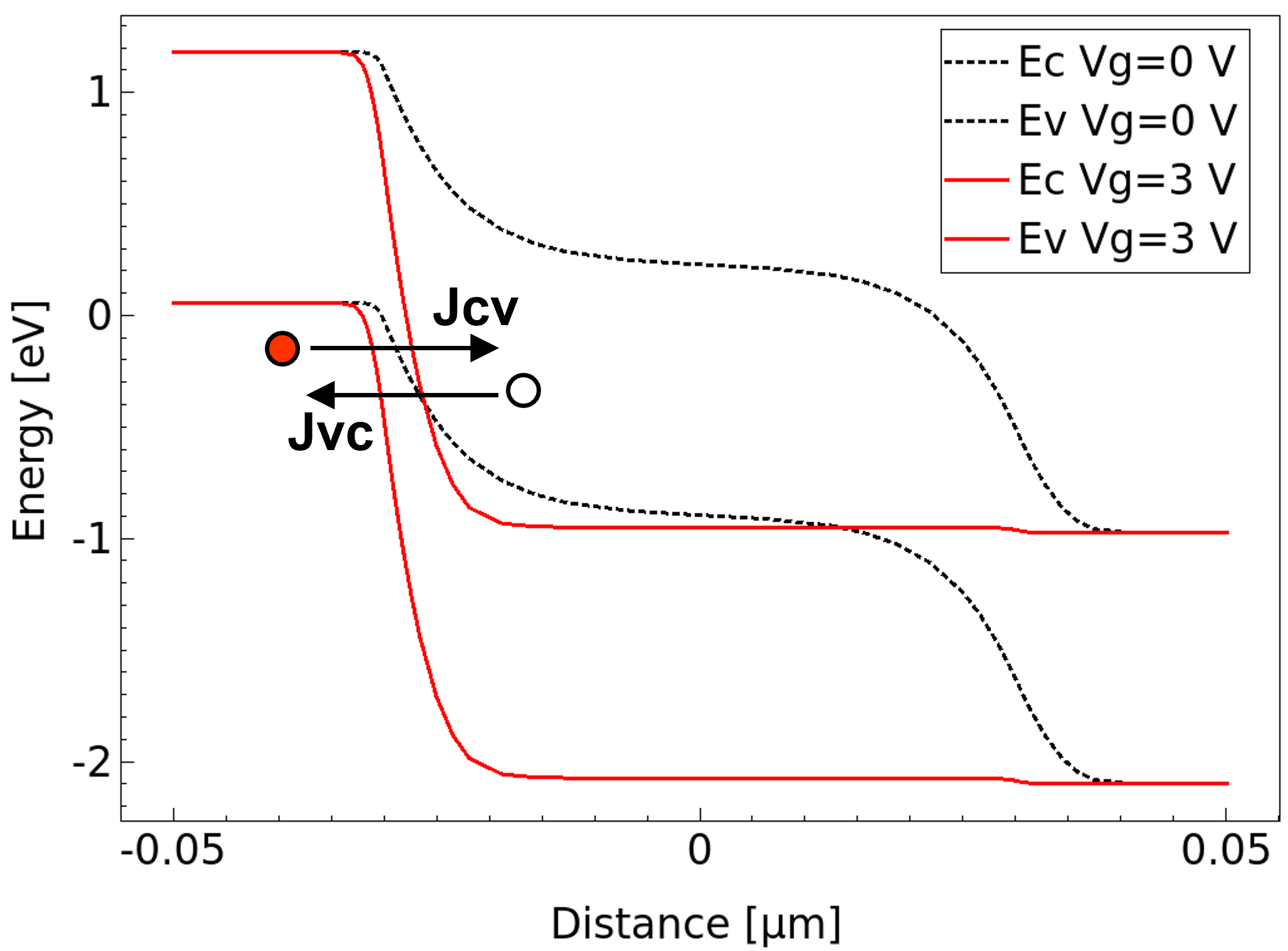
Figure 40. Operation of tunnel FET. (Click image for full-size view.)
The project (TunnelFET) includes structure generation and Id–Vg simulation. You are encouraged to modify the Sentaurus Device command file to account for band-to-band tunneling.
The complete project can be investigated from within Sentaurus Workbench in the directory Applications_Library/GettingStarted/sdevice/Tunneling/TunnelFET.
main menu | module menu | << previous section | next section >>
Copyright © 2024 Synopsys, Inc. All rights reserved.