
Sentaurus Device
13. Special Focus: Traps
13.1 Trap Types
13.2 Defining Traps
13.3 Types of Trap Density-of-States
13.4 Trap Spatial Distribution
13.5 Trap Occupation
13.6 Trap Cross-Section
13.7 Poole-Frenkel Model for Cross Sections
13.8 Trap as Doping
13.9 Trap Fill Controls
13.10 Trap Visualization
Objectives
- To demonstrate how to work with traps in simulations using Sentaurus Device.
13.1 Trap Types
Traps are very important physical quantities that can drastically affect the electrical performance of a device. They act similarly to dopings, supplying free carriers, enhancing recombination, increasing leakage, and (when charged) also contributing to a total charge in the right-hand side of the Poisson equation, thereby influencing device electrical behavior.
In Sentaurus Device, different trap objects are considered:
- Rechargeable bulk and interface traps, energetically distributed inside a semiconductor or an insulator material band gap
- Fixed charges, distributed inside an insulator bulk material or at arbitrary material interfaces
For rechargeable traps, two trap types are available:
- An Acceptor (or eNeutral) trap that is uncharged when unoccupied and becomes negatively charged when capturing an electron.
- A Donor (or hNeutral) trap that is uncharged when unoccupied and becomes positively charged when capturing a hole.
For both trap types, electron–hole recombination through such a trap is allowed.
There is no default trap type. Therefore, you must specify a trap type explicitly.
Another available species is the fixed charge, which is a trap fully occupied by either electrons or holes. Therefore, its charge stays constant throughout the entire simulation and does not depend on electrical bias conditions. Electron–hole recombination through such a trap is not allowed. This type of trap uses the FixedCharge keyword for a trap specification.
Both rechargeable and fixed-charge traps can be specified at the bulk or at any material interface.
13.2 Defining Traps
Traps can be defined globally, materialwise, regionwise, or interface-wise.
The following template shows the materialwise definition of a bulk trap:
Physics (Material="<material_name>") {
  Traps(
    ( <trap_type> Conc=<value>
     [<trap_DOS_type>
      <trap_cross_section>
      <trap_tunneling_parameters>])
    (...)
  )
}
where Conc represents a trap concentration. Other trap-related parameters are explained later. As many traps as needed can be specified inside a single Traps section.
In the case of a bulk trap, its concentration is given in cm-3 or cm-3 eV-1. For interface traps, it is given in cm-2 or cm-2 eV-1, depending on the type of trap density-of-states (see Section 13.3 Types of Trap Density-of-States).
Here is an example of the global specification of a rechargeable bulk trap:
Physics {
  Traps(
    (eNeutral Level fromMidBandGap EnergyMid=0.
     Conc=1e15 eXsection=1e-10 hXsection=1e-10)
  )
}
Similar syntax is applied for an interface trap specification:
Physics (MaterialInterface= "<Material_1>/<Material_2>" ) {
  Traps(
    ( <trap_type> Conc=<value>
     [<trap_DOS_type>
      <trap_cross_section>
      <trap_tunneling_parameters>])
    (...)
  )
}
The following example shows the typical syntax for an interface fixed-charge trap specification at material interfaces:
Physics (MaterialInterface= "Silicon/Oxide" ) {
  Traps (FixedCharge Conc=-1e11)
}
For the FixedCharge trap type, the sign of Conc denotes the sign of the fixed charges.
13.3 Types of Trap Density-of-States
The trap energy distribution inside a material band gap is defined in the Traps section by specifying any of the available trap density-of-states (DOS):
- Level represents a single-energy trap level at a predefined EnergyMid position. Trap concentration is given in cm-3 (bulk traps) or cm-2 (interface traps).
- Uniform represents a uniformly energy-distributed trap inside a material band gap, controlled by the energy reference point, EnergyMid and EnergySig parameters. Trap concentration is given in cm-3 eV-1 (bulk traps) or cm-2 eV-1 (interface traps).
- Exponential represents an exponentially energy-distributed trap inside a material band gap, controlled by the energy reference point, EnergyMid and EnergySig parameters. Trap concentration is given in cm-3 eV-1 (bulk traps) or cm-2 eV-1 (interface traps).
- Gaussian represents a Gaussian energy-distributed trap inside a material band gap, controlled by the energy reference point, EnergyMid and EnergySig parameters. Trap concentration is given in cm-3 eV-1 (bulk traps) or cm-2 eV-1 (interface traps).
- Table specifies a tabular trap energy distribution. Trap concentration is given in cm-3 eV-1 (bulk traps) or cm-2 eV-1 (interface traps).
There is no default trap DOS type. Therefore, you must specify it explicitly.
The following example shows the trap energy distribution–related syntax:
Traps(
  (...
   <trap_DOS_type>
   <energy_reference_point>
   EnergyMid=<E0>
   EnergySig=<Es>
  )
)
For the energy reference point, any of the following keywords can be used:
- FromConBand selects a material conduction band edge as a reference point.
- FromValBand selects a material valence band edge as a reference point.
- FromMidBandGap selects the middle of a semiconductor material band gap as a reference point.
The following example defines the eNeutral level-type trap located exactly in the middle of a material band gap:
Physics {
  Traps(
    (eNeutral Level fromMidBandGap EnergyMid=0.
     Conc=1e15 eXsection=1e-10 hXsection=1e-10)
  )
}
The complete project that demonstrates different definitions of trap DOS types can be investigated from within Sentaurus Workbench in the directory Applications_Library/GettingStarted/sdevice/Traps/TrapDOS.
Click to view the primary file sim1_des.cmd.
This file shows how different trap DOS specifications can be activated, where the DOS project parameter is used to select a trap DOS type.
To plot the trap density versus energy distribution, the TrappedCarDistrPlot section is used in the project. In this section, you must specify the exact locations of traps within a material or region, where the trap data will be plotted:
TrappedCarDistrPlot {
        Material="Silicon"{(0. 0.)}
}
Figure 1 shows the results of this command.
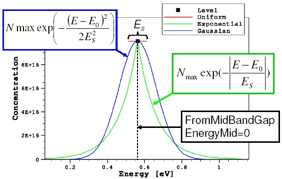
Figure 1. Trap DOS energy distributions for different definitions of trap DOS.
13.4 Trap Spatial Distribution
By default, traps are distributed uniformly inside a material or at a material interface. You can have a spatially nonuniformly distributed trap profile using:
- The SFactor specification
- The SpatialShape specification
In this section, you will use both the approaches to define a spatially varying trap profile. The corresponding Sentaurus Workbench project can be found in the directory Applications_Library/GettingStarted/sdevice/Traps/TrapSpatial. The Sentaurus Workbench parameters spatial_dist and case are used to refer to various simulation cases discussed herein.
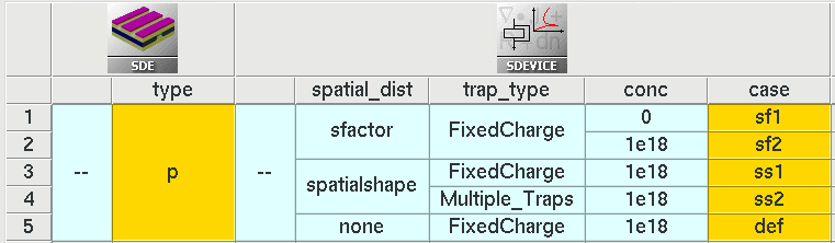
Figure 2. Sentaurus Workbench view noting various simulation cases. (Click image for full-size view.)
The SFactor specification: Here, the spatially varying trap profile is specified using the SFactor keyword inside the Trap section of the command file:
Traps( (... SFactor= "<dataset_name>") )
Here, <dataset_name> indicates the external data field on which the trap spatial nonuniformity is based.
Limited dataset names are allowed in the SFactor specification, such as DeepLevels, xMoleFraction, and yMoleFraction (read from the doping file), eTrappedCharge and hTrappedCharge (read from the file specified by DevFields in the File section), or PMI user fields PMIUserField0...10 (read from the file specified by PMIUserFields in the File section).
It represents the concept of how to introduce a nonuniform 2D spatial trap distribution. The project involves Sentaurus Structure Editor and Sentaurus Device.
Sentaurus Structure Editor defines the device geometry and doping profile. In addition, it defines the nonuniformly distributed function, called DeepLevels. Mesh generation is performed inside Sentaurus Structure Editor by directly calling Sentaurus Mesh.
Sentaurus Device defines the nonuniform traps, applying the SFactor specification to the trap definition, which refers to the DeepLevels dataset name.
Click to view the primary file sim1_des.cmd.
The DeepLevels dataset name is taken from the Grid file, which is specified in the File section, while trap_type and conc are the project parameters:
File {
  grid    = "@tdr@"
...
}
Physics {
  Traps(
    (@trap_type@ Conc=@conc@ SFactor="DeepLevels")
  )
}
Two values are assigned to the conc parameter: 0 and \(10^{18}\). Having the conc parameter value set to zero indicates to Sentaurus Device that the specified dataset determines the spatial distribution directly. For a nonzero conc parameter value, the resulting distribution is scaled according to the following formula:
\[N_{\text"trap"}(x,y) = \text"conc" · {\text"DeepLevels"(x,y)} / {\text"DeepLevels"(\text"max")} \]
where \(\text"DeepLevels"(\text"max")\) refers to the DeepLevels dataset peak value.
Figure 3 shows the resulting trapped hole concentration profiles.
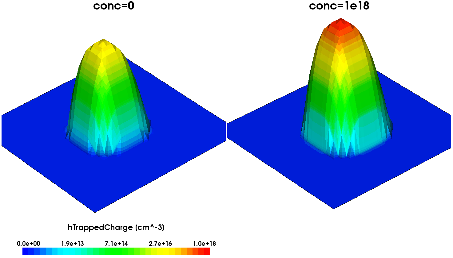
Figure 3. Trapped hole density distributions plotted for (left) conc=0 and (right) conc=1e18 trap specifications. (Click image for full-size view.)
The following syntax illustrates the definition of an acceptor-type interface trap spatial distribution, based on the PMIUserField0 dataset, loaded from the external abc.tdr file:
File {
  ...
  PMIUserFields = "abc.tdr"
}

Physics(MaterialInterface="Silicon/Oxide"){
  Traps(
    Acceptor Conc=1e11 Gaussian fromMidBandGap EnergyMid=0. EnergySig=0.1
    SFactor="PMIUserField0"
  )
}
The SpatialShape specification: Here, the spatially varying trap profile is specified using the SpatialShape keyword inside the Trap section of the command file. The SpatialShape keyword selects a multiplicative modifier function for the trap concentration. You will understand these aspects by using some examples. The following example (case=def) specifies a fixed charge with concentration 1e18 cm-3. This results in a spatially uniform trap distribution of fixed charge (see Figure 4(a)), which is the default behavior because no explicit spatial trap variation is specified).
Physics {
  Traps(
    (FixedCharge Conc=1e18)
  )
}
For case=ss1, the following syntax specifies a spatially uniform (box shaped) fixed charge with a concentration of 1e18 cm-3 at vertex SpaceMid=(-0.2,-0.2) and extending SpaceSig_x=0.04μm on either side of x=–0.2 along x-axis and extending SpaceSig_y=0.08 μm on either side of y=–0.2 along y-axis. The resulting trap profile is shown in Figure 4(b).
Physics {
  Traps(
    (name="t1" FixedCharge Conc=1e18
      SpatialShape= Uniform SpaceMid=(-0.2,-0.2,0) SpaceSig=(0.04,0.08,100))
  )
}
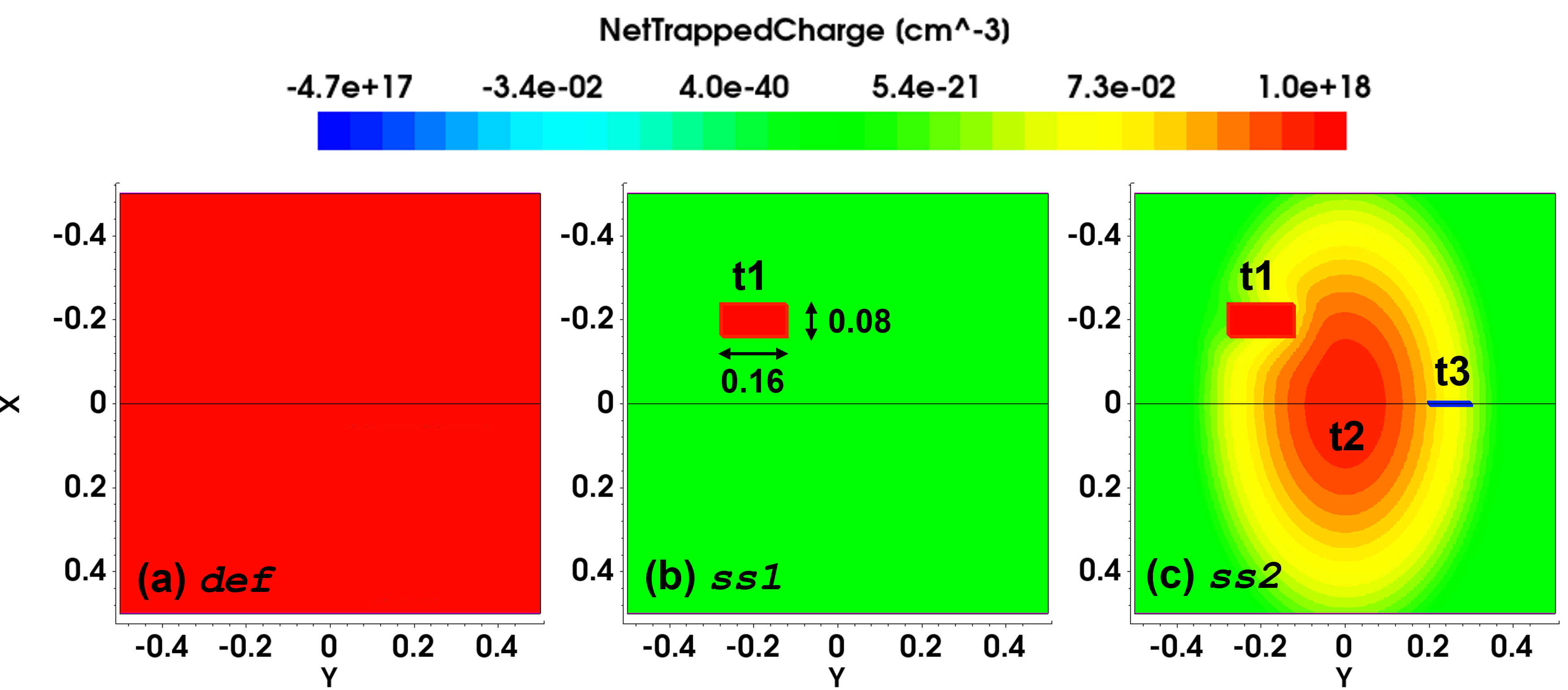
Figure 4. Net trapped charge for (a) uniform spatial distribution in the entire region (case=def), (b) uniform box spatial distribution (case=ss1), and (c) multiple spatially varying trap specifications t1, t2 and t3 (case=ss2). (Click image for full-size view.)
For case=ss2, the following syntax specifies three spatially varying traps t1, t2, and t3 and the resulting net trapped charge profile is shown in Figure 4(c). The trap t1 is the same as that of ss1. The trap t2 specifies a spatially varying Gaussian profile with peak at SpaceMid=(0,0) and standard deviations of SpaceSig_x=0.04μm and SpaceSig_x=0.025μm along x-axis and y-axis respectively. The trap t3 specifies uniform line-shaped spatial distribution for the interface "region_1/region_2" (see Figure 4(c), t3).
  Physics {
    Traps(
      (name="t1" FixedCharge Conc=1e18
        SpatialShape= Uniform SpaceMid=(-0.2,-0.2,0) SpaceSig=(0.04,0.08,100))
      (name="t2" hNeutral Conc=1e18 EnergyMid=0
        SpatialShape= Gaussian SpaceMid=(0,0,0) SpaceSig=(0.04,0.025,100))
    )
  }

  Physics (RegionInterface="region_1/region_2"){
     Traps(
      (name="t3" eNeutral Conc=1e13 EnergyMid=0
        SpatialShape= Uniform SpaceMid=(0,0.25,0) SpaceSig=(100,0.05,100))
     )
  }
13.5 Trap Occupation
Trap charges are computed by multiplying the trap occupation by the trap concentration. Trap occupation is independent of the trap concentration and depends on the Fermi level and trap energy together with various capture or emission rates, corresponding to various capture or emission processes.
Each capture and emission process couples the trap to a reservoir of carriers. If only a single process would be effective, in the stationary state, then the trap would be in equilibrium with the reservoir for this process. This consideration (the principle of detailed balance) relates capture and emission rates:
Figure 5 shows three groups of capture and emission processes typical for semiconductor devices:
- Local capture and emission
- Nonlocal elastic tunnel capture and emission (based on nonlocal mesh)
- Nonlocal inelastic phonon-assisted tunnel capture and emission (based on nonlocal mesh)
Figure 5. Different capture and emission processes. (Click image for full-size view.)
Without nonlocal tunneling for traps, only local exchange of carriers with both the bands is considered (processes 1 and 2 in Figure 5). Processes 1 and 2 are relevant only for semiconductors and not for insulators as Sentaurus Device does not solve the current continuity equations in insulators.
The following expressions summarize the local capture/emission model and related parameters.
For a brief introduction to nonlocal capture/emission models, see Section 19. Special Focus: Traps, 19.2.5 Nonlocal Tunneling for Traps.
Specify TrappingRates in the Plot section to see the capture and emission rates for each trap, split into local processes (TotalLocalCapture and TotalLocalEmission), inelastic tunneling processes (TotalInelasticCapture and TotalInelasticEmission), and elastic tunneling processes (TotalElasticCapture and TotalElasticEmission).
Trap occupation dynamically changes due to carrier capture or emission by or from a trap. As mentioned earlier, Sentaurus Device allows you to plot a trap-energy distribution and occupation using the TrappedCarDistrPlot section in the input.
The specification inside the TrappedCarDistrPlot section defines a trap spatial location within a specified material, at which a trap distribution or occupation must be plotted. Resulting trapped charge density, trap occupation probability, and trap density quantities as functions of energy are saved in a file indicated by the TrappedCarPlotFile keyword in the File section.
The Applications_Library/GettingStarted/sdevice/Traps/TrapOccupation project demonstrates the consequence of varying the Gaussian DOS trap-level peak position inside the silicon material band gap.
Click to view the primary file sim1_des.cmd.
The quasi-Fermi-level position is established by the uniformly distributed p-type doping with a concentration of 1017 cm–3. The eNeutral trap-type energy position within the band gap is controlled by the shift parameter, whose value varies between -0.4 eV and 0.3 eV, having the silicon mid–band gap as a reference point:
Physics {
  ...
  Traps(
    (@trap_type@ Gaussian fromMidBandGap
     Conc=1e17 EnergyMid=@shift@ EnergySig=0.1
     eXsection=1e-8 hXsection=1e-8)
  )
}
Figure 6 shows the resulting trap-density energetic distributions. Figure 7 shows the corresponding trapped charge densities as well as their occupation probability as a function of energy. The corresponding electron quasi-Fermi-level position is indicated by a vertical green line.
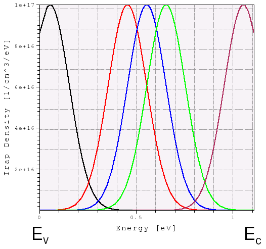
Figure 6. Trap density variations in energy space for different energy-peak displacement values, which move the trap-energy reference point from the mid–band gap towards the conduction or valence band edges. (Click image for full-size view.)
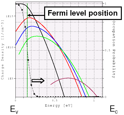
Figure 7. Trapped charge-density variations in energy space corresponding to the trap densities shown above. The trap occupation probability is indicated by the black-dotted curve and is established by the quasi-Fermi-level position (vertical green line). As can be seen, shallower traps capture more carriers than traps located far away from the valence band edge. (Click image for full-size view.)
13.6 Trap Cross-Section
The trap cross-section is the key parameter that defines the charge-trapping dynamics and the carrier recombination rate through a trap. The effective trap time constant (the time required for a single-trapping or de-trapping event) can be estimated as:
\[ τ_{\text"eff"} = {1}/{N_t \ v_{\text"th"}·σ} \]
where \(N_t\) is the trap level concentration, \(v_{\text"th"}\) is the thermal velocity, and \(σ\) is the trap cross-section.
For example, for \(N_t = 10^{17}\) cm-3, \(v_{\text"th"} = 2·10^7\) cm/s, and \(σ = 10^{-14}\) cm-2, the estimated trap lifetime \(τ_{\text"eff"}\) is \(5·10^{-11}\) s.
While in the case of a transient simulation, the carrier trap capture and emission are described by the detailed balance equation, under the steady-state assumption, the net carrier recombination through a single trap level is represented as:
\[ R_{\text"net"} = {N_0\ v_{\text"th"}^n\ v_{\text"th"}^p\ σ_n\ σ_p ( np - n_{i,\text"eff"}^2 )}/ {v_{\text"th"}^n\ σ_n ( n+n_1/g_n)+v_{\text"th"}^p\ σ_p ( p+p_1/g_p)} \]
where \(N_0\) denotes the trap concentration, and the \(n\) and \(p\) indexes correspond to electrons and holes.
Assuming equal electron and hole trap cross-sections and unit degeneration factors \(g_n = g_p = 1\), the above formula can be represented in a form of the well-known SRH approximation:
\[ R_{\text"net"}^{\text"SRH"} = {np-n_{i,\text"eff"}^2}/{τ_p (n + n_1) + τ_p (p + p_1)} \]
where \(τ_n\) and \(τ_p\) represent effective carrier lifetimes, and the \(n_1\) and \(p_1\) parameters implicitly take a trap-level energy into consideration.
The Applications_Library/GettingStarted/sdevice/Traps/TrapRecombination project demonstrates the influence of the trap cross-section value on a p-n junction leakage current under reverse bias condition. The trap cross-section for a specified eNeutral trap is varied as the Xsec project parameter.
Click to view the primary file sim1_des.cmd.
Under the reverse bias condition, the p-n junction is fully depleted of carriers, thereby resulting in a strong carrier generation inside the depleted region (see Figure 8). This causes the higher leakage current in the case of a higher trap cross-section value, as shown in Figure 9.
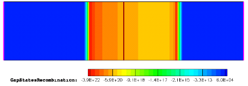
Figure 8. Gap-state recombination rate distribution inside a p-n junction structure, taken at –100 V bias. Negative recombination rate values represent the carrier generation.
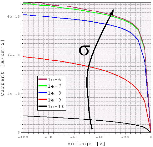
Figure 9. Reverse diode I–Vs calculated with different bulk trap cross-section values. Higher leakage is observed for the higher trap cross-section.
The highest recombination through a trap level is achieved if a trap is positioned in the middle of the semiconductor material band gap, where the electron- or hole-capturing probabilities are the highest as shown in Figure 10.
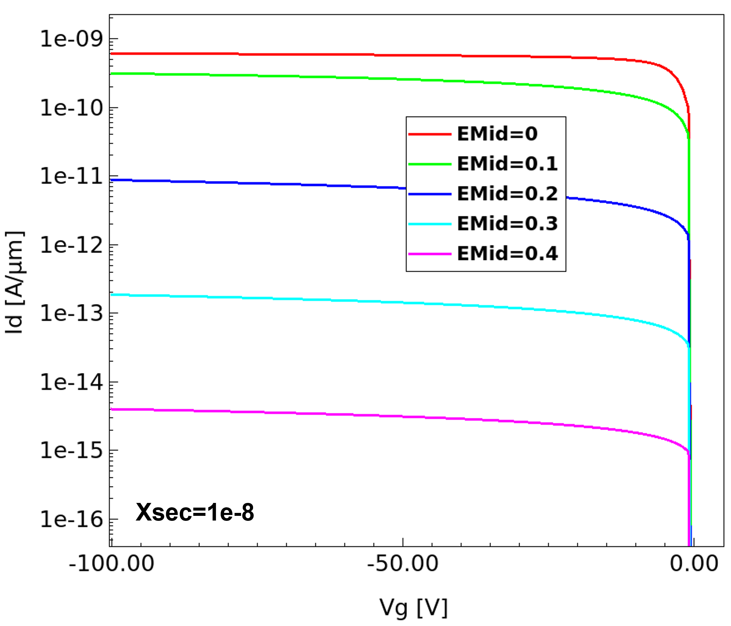
Figure 10. Reverse diode I–Vs calculated with different trap energy level values. Higher leakage is observed for the traps close to the mid bandgap. (Click image for full-size view.)
13.7 Poole-Frenkel Model for Cross Sections
As mentioned earlier, trap occupation depends on the Fermi level and trap energy together with various capture and emission rates. Capture and emission rates are either local or nonlocal (corresponding to nonlocal mesh based tunneling). The capture and emission rates further depend on cross sections. By default, the cross sections are constant which are set by eXsection and hXsection keywords as discussed in Section 13.5 Trap Occupation.
Sentaurus Device offers different models for cross sections and the Poole–Frenkel model is frequently used to interpret transport effects in dielectrics and amorphous films. The Poole–Frenkel model predicts the enhanced emission rate of carriers in an external electric field due to the lowering of the potential barrier.
This section discusses the Poole-Frenkel Model for cross sections and applies it for simulating reverse current characteristics of a pn diode.
The complete project can be investigated from within Sentaurus Workbench in the Applications_Library/GettingStarted/sdevice/Traps/TrapXsec_PooleFrenkel directory.
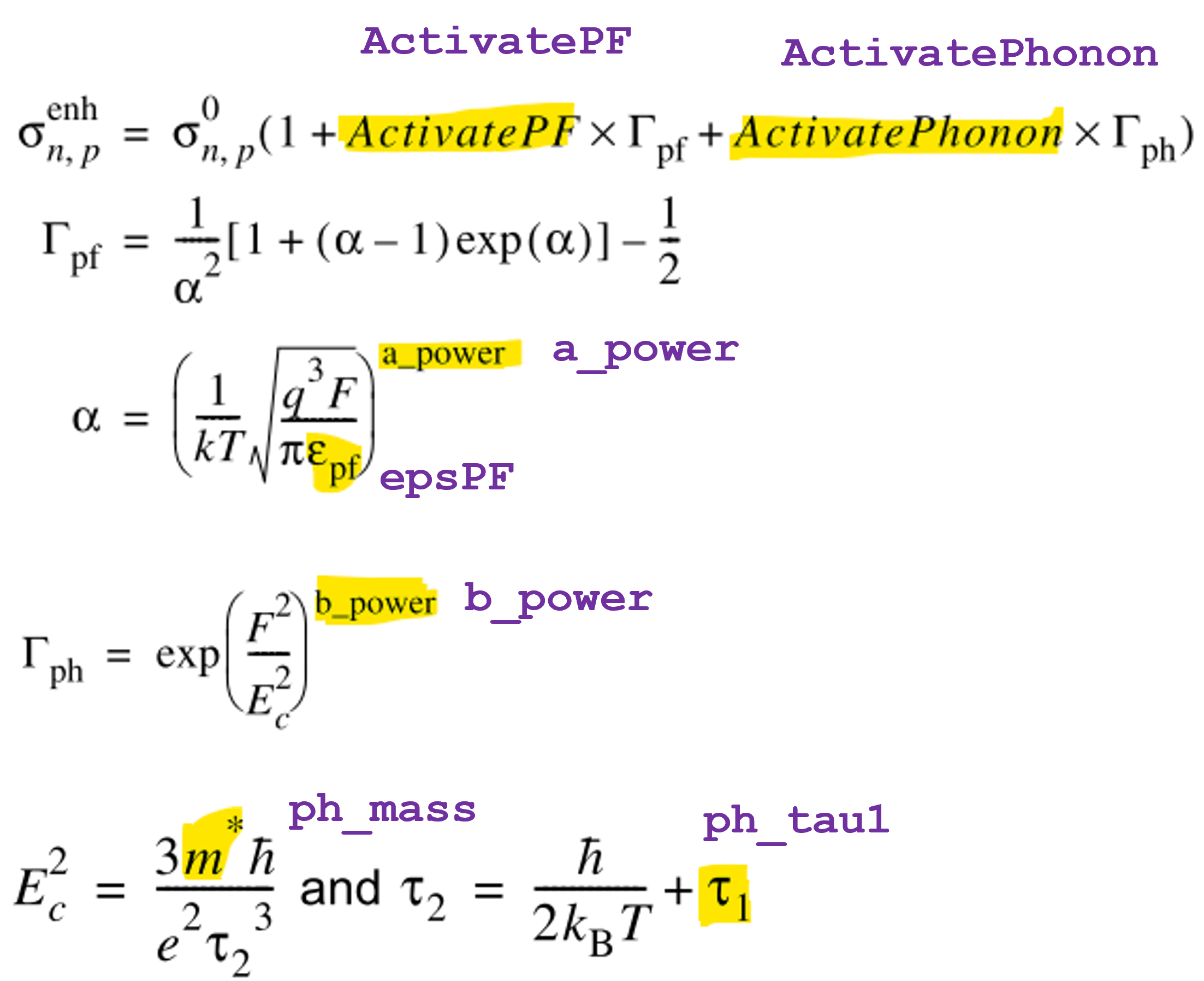
The following expressions summarize the field enhancement of cross sections, noting the parameters that can be modified in the parameter file. The ActivatePF and ActivePhonon parameters are the activating and scaling factors for the two components of the Poole–Frenkel enhancement; 1) Poole–Frenkel and 2) phonon assisted tunneling.
The model can be activated by specifying the PooleFrenkel keyword in the Traps specification of the command file:
The specification of model parameters is optional. The default parameter set is used if the parameter set is not modified. The parameters can be modified in the PooleFrenkel parameter set. The default parameter set is shown here for reference.
  PooleFrenkel
  {
     ActivatePF  =  1,   1
     a_power = 1, 1
     epsPF	= 11.7,	11.7

     ActivatePhonon = 0, 0
     b_power = 1, 1
     ph_mass = 0.25 , 0.4
     ph_tau1 = 5e-15 , 5e-15
  }
The trap specification shown below is used for the pn diode structure shown in Figure 11 (left). The simulation with Poole–Frenkel model is
compared to the reference case (ref) with constant cross sections. Figure 11 (right) shows the enhanced trap local emission rate
for the Poole–Frenkel model compared to the ref.
  Traps(
    (eNeutral Level fromMidBandGap
     Conc=1e15 EnergyMid=0.4 EnergySig=0.01
     eXsection=1e-8 hXsection=1e-8
     PooleFrenkel
    )
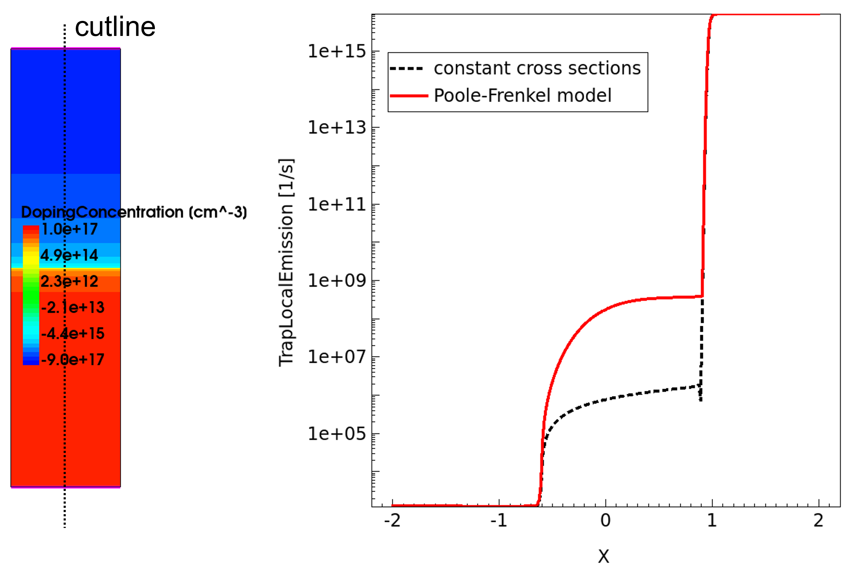
Figure 11. The pn diode structure (left) used for simulation and trap local emission rates with constant cross sections (dotted) and field-enhanced Poole-Frenkel cross sections for Vd=–100 V. (Click image for full-size view.)
Figure 12 shows the increased reverse diode current for the Poole–Frenkel model compared to the ref case.
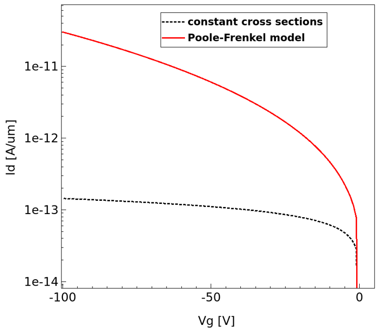
Figure 12. Reverse diode I–Vs with constant cross sections (dotted) and field enhanced Poole-Frenkel cross sections (solid). (Click image for full-size view.)
Figure 13(a) shows the contribution for the two components of Poole–Frenkel model on reverse diode current. The component corresponding to ActivatePF=1 is the dominant of the two components for the default parameter set. Figure 13(b) shows the effect of a_power on reverse diode current.
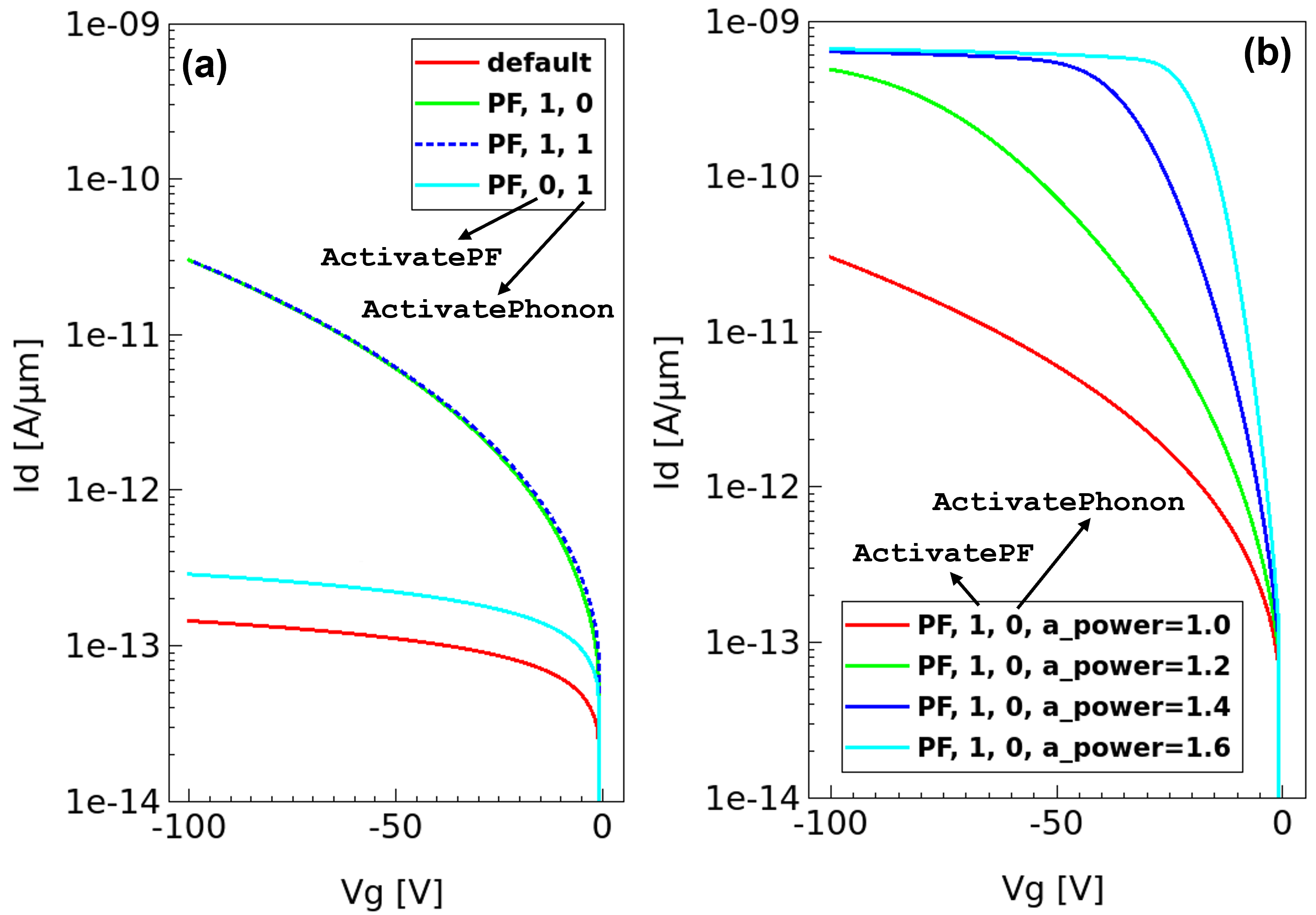
Figure 13. Reverse diode I–Vs: (a) The two components of Poole-Frenkel model activated using ActivatePF and ActivePhonon parameters. (b) Effect of Poole-Frenkel parameter a_power. (Click image for full-size view.)
13.8 Trap as Doping
Charged traps also act like scattering centers (similar to doping), so their influence on carrier kinetics must be accounted for when using doping-dependent carrier mobility. To add a trap to the doping concentrations, specify the keyword Add2TotalDoping in the Trap section in combination with an appropriate mobility-doping dependency model, for example:
  Physics {
    Mobility( DopingDep )     * turns on mobility doping dependency
    Traps(
      ( Donor                 * electron trap level (synonym of eNeutral)
...
Add2TotalDoping
    )
  )
}
The Applications_Library/GettingStarted/sdevice/Traps/Trap2Doping project demonstrates how this option activation affects carrier mobility.
Click to view the primary file sdevice_des.cmd.
Figure 14 illustrates the hole mobility dependency on doping concentration, having different combinations of doping and trap specifications.
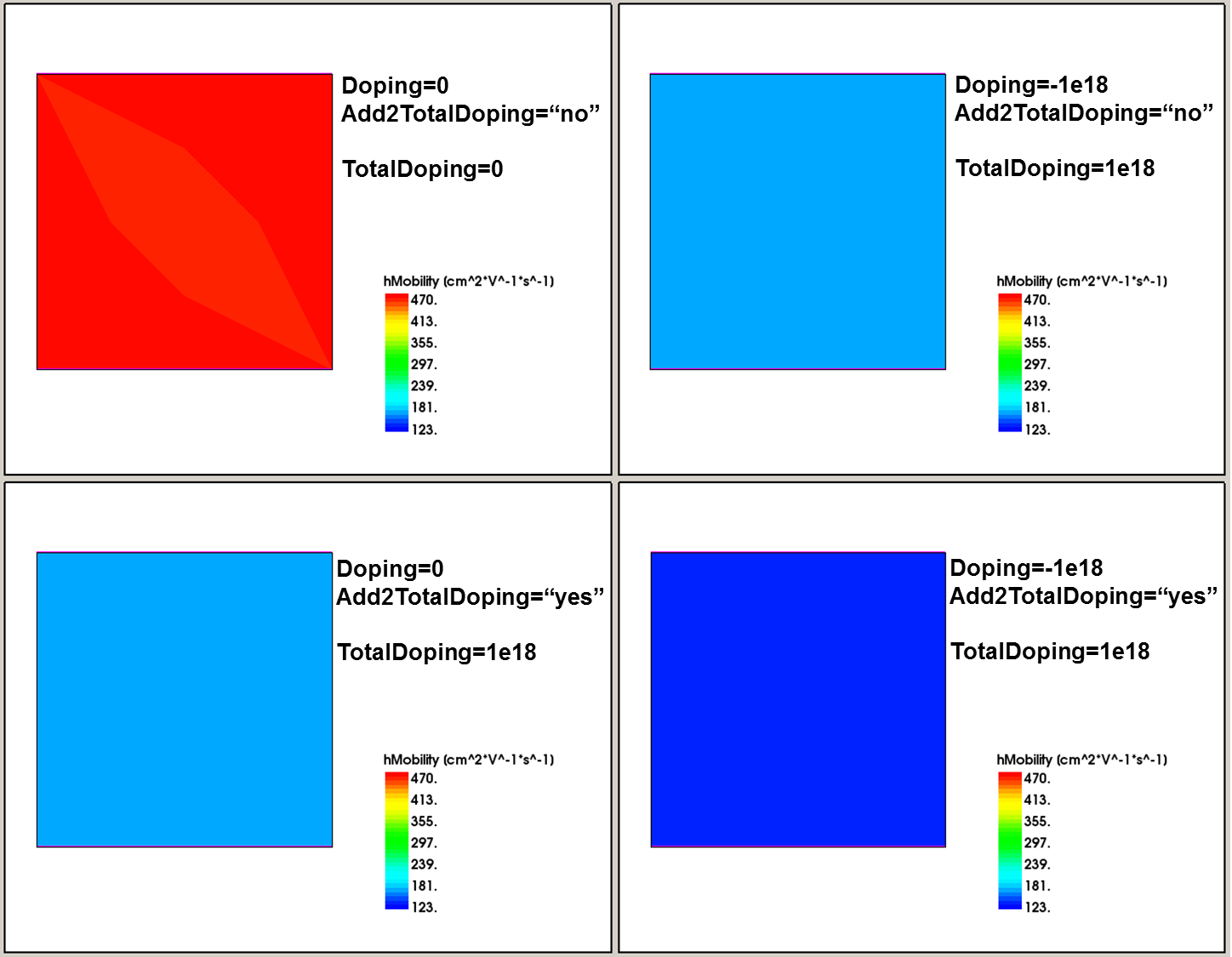
Figure 14. Hole bulk-mobility variation with different combinations of doping and trap specifications. In all cases, the 1e18 cm-3 donor trap concentration is defined. (Click image for full-size view.)
13.9 Trap Fill Controls
Under certain circumstances, it can be useful to define a trap occupancy explicitly. Sentaurus Device provides such a capability using trap fill controls, which use an explicit way to specify a trap occupation. Trap fill controls are specified in the Solve section, for example:
Solve {
  Set (TrapFilling=Empty)
  Quasistationary {...}
  UnSet (TrapFilling)
  Transient {...}
}
In this example, the first Set statement sets all traps as empty (not charged). After the Quasistationary simulation, the UnSet (TrapFilling) statement releases all traps to their actual state, which are used in the subsequent Transient simulation.
The available trap fill controls are:
- Set (TrapFilling=Full) sets all traps as fully occupied.
- Set (TrapFilling=Empty) sets all traps as empty.
- Set (TrapFilling=0) provides a trap occupation for the n=p=0 condition.
- Set (TrapFilling=n), Set (TrapFilling=p) sets a trap occupation to be in equilibrium with a very high n(p) concentration and zero p(n) concentration.
- Set (TrapFilling=Frozen) provides unchanged (from previous step) trap occupation.
- UnSet (TrapFilling) resets any of these controls and switches on the regular trap-filling dynamics.
The Applications_Library/GettingStarted/sdevice/Traps/FillControls project demonstrates the consequence of using different trap fill controls.
Click to view the primary file sim1_des.cmd.
13.10 Trap Visualization
To visualize trap-related quantities in Sentaurus Visual, the following keywords can be specified in the Plot section of the Sentaurus Device command file:
Plot {
 eTrappedCharge           * plots electron concentration trapped on eNeutral
                          * and Acceptor traps
 hTrappedCharge           * plots hole concentration trapped on hNeutral
                          * and Donor traps
 eInterfaceTrappedCharge  * plots electron concentration trapped in eNeutral
                          * and Acceptor interface traps
 hInterfaceTrappedCharge  * plots hole concentration trapped in hNeutral and
                          * Donor interface traps
 TotalTrapConcentration   * plots total bulk trap concentration
 TotalTrapConcentration/RegionInterface  * plots the absolute value of the net
					   interface trap concentration; does
					   not account for trap occupancy
 eTrapConcentration	  * plots absolute value of bulk trap concentration
 			    for eNeutral and Acceptor traps
 hTrapConcentration	  * plots absolute value of bulk trap concentration
 			    for hNeutral and Donor traps
 TotalInterfaceTrapConcentration  * plots total interface trap concentration;
 				    stored as a bulk quantity with a nonzero
                                    value only on interfaces
 TrapConcentration 	  * plots trap concentrations for each energy level
 			    of each trap entry specified in the command file
 eGapStatesRecombination  * plots electron recombination rate through traps
 hGapStatesRecombination  * plots hole recombination rate through traps
 TrappingRates            * plots local capture/emission rates
                            (TotalLocalCapture, TotalLocalEmission)
                            and nonlocal capture/emission rates
                            (TotalInelasticCapture, TotalInelasticEmission,
                            TotalElasticCapture and TotalElasticEmission)
}
The eTrappedCharge and hTrappedCharge datasets include the contribution of interface charges as well. To this end, Sentaurus Device converts the interface densities to volume densities and, therefore, their contribution depends on the mesh spacing. To plot interface charges separately as interface densities, use eTrappedCharge/RegionInterface and hTrappedCharge/RegionInterface.
For the visualization of the trapped carrier charge density, the trap occupancy probability, and the trap density distribution in energy space, see Section 13.5 Trap Occupation for details.
Copyright © 2024 Synopsys, Inc. All rights reserved.