 main menu
| module menu
| << previous section
| next section >>
main menu
| module menu
| << previous section
| next section >>
Sentaurus Workbench
11. Sentaurus Device Wizard
11.1 Overview of Sentaurus Device Wizard
11.2 Using the Sentaurus Device Wizard
11.3 Supported Application Examples
Objectives
- To demonstrate how to use the Sentaurus Device Wizard.
11.1 Overview of Sentaurus Device Wizard
The Sentaurus Device Wizard offers custom solutions for Sentaurus Device input generation, followed by visualization of results and parameter extraction with Sentaurus Visual.
The Sentaurus Device Wizard is designed to help TCAD users to:
- Mitigate the rigidity of the constructions of the Sentaurus Device input language, and make it easier for beginners to use
- Provide ready-to-go application examples for most frequently used TCAD applications
- Reduce the overall complexity of setting up a device simulation flow in Sentaurus Workbench
The Sentaurus Device Wizard consists of two parts:
- The graphical user interface (GUI)
- The library of examples, where examples are grouped by applications. Each application group typically represents either certain device functionality (such as power, wide bandgap, and memory devices) or different simulation techniques (such as degradation, radiation, noise, and variability). Each example is already equipped with the corresponding TDR geometry, which is referred to in the corresponding Grid input statement (see Section 1.2.1 File Section).
11.2 Using the Sentaurus Device Wizard
To create an input command file for Sentaurus Device:
- Create a new project and add the Sentaurus Device tool in it.
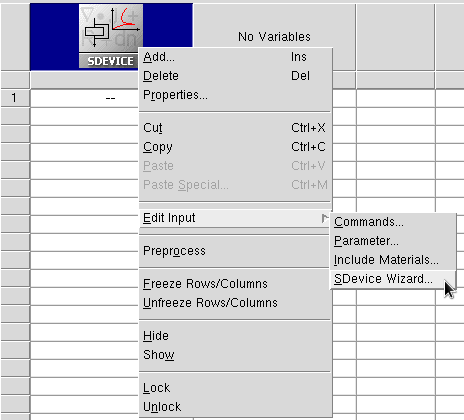
- Choose Tool > Edit Input, or
right-click the Sentaurus Device tool icon and choose Edit Input > SDevice Wizard.
The Sentaurus Device Wizard opens.
The following chart shows the operational scenario of the wizard, where you make several selections and enter your input as required. Some selections such as Physical Models and Numerical Setting can be omitted.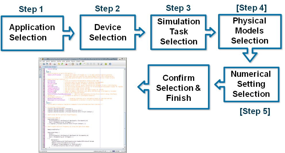
- Select an application.
For example, under Special Technique Demonstrators, select Breakdown Simulation.
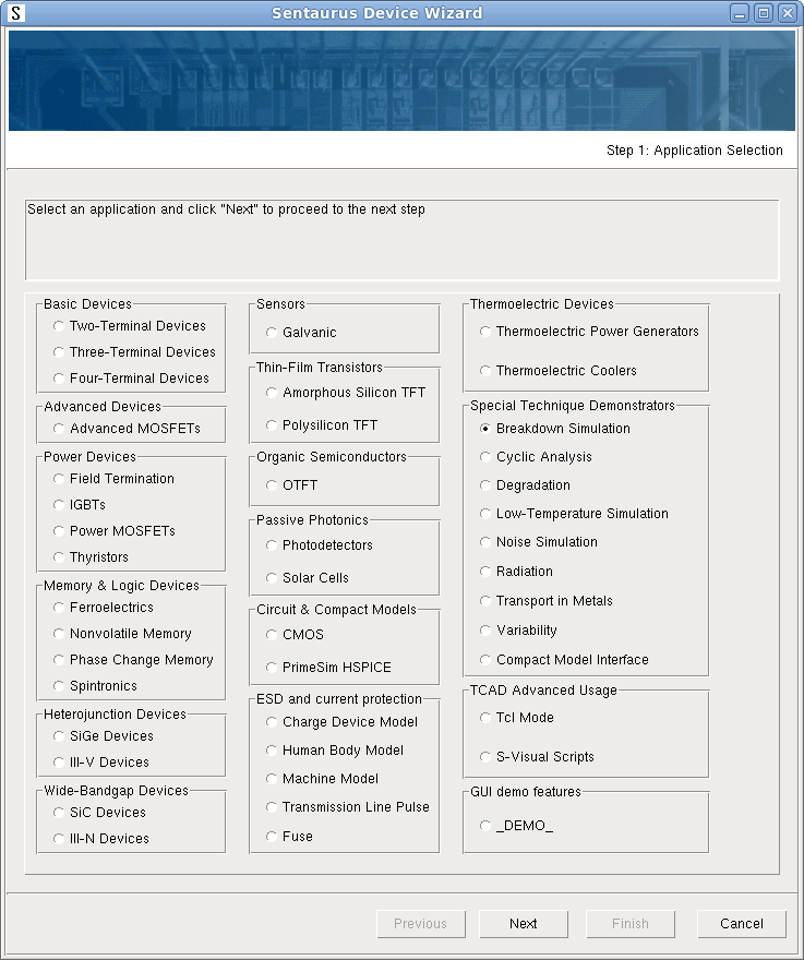
- Click Next.
- Select a device (only one device is available for this application).
The options available depend on the application previously selected.
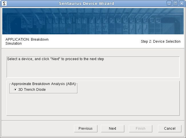
- Click Next.
- Select a simulation task.
Two tasks are available for the selected device. Select Diode reverse bias ramp with ABA.
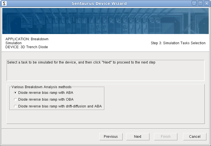
- Click Next.
- Select the numeric control parameter values and other controls.
These options provide the possibility to generate commented input and select a tool name for the Sentaurus Visual tool instance.
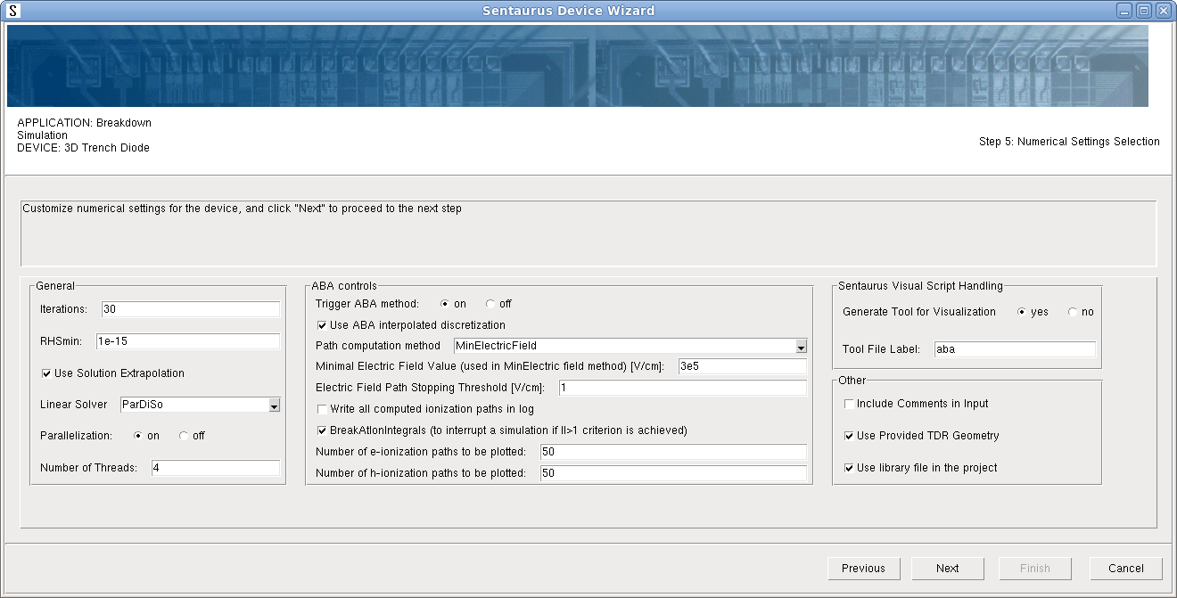
- Click Next.
- At the end, review the selection summary, which shows all the chosen settings for the
selected simulation task including physical models and numeric parameters for the
selected device.
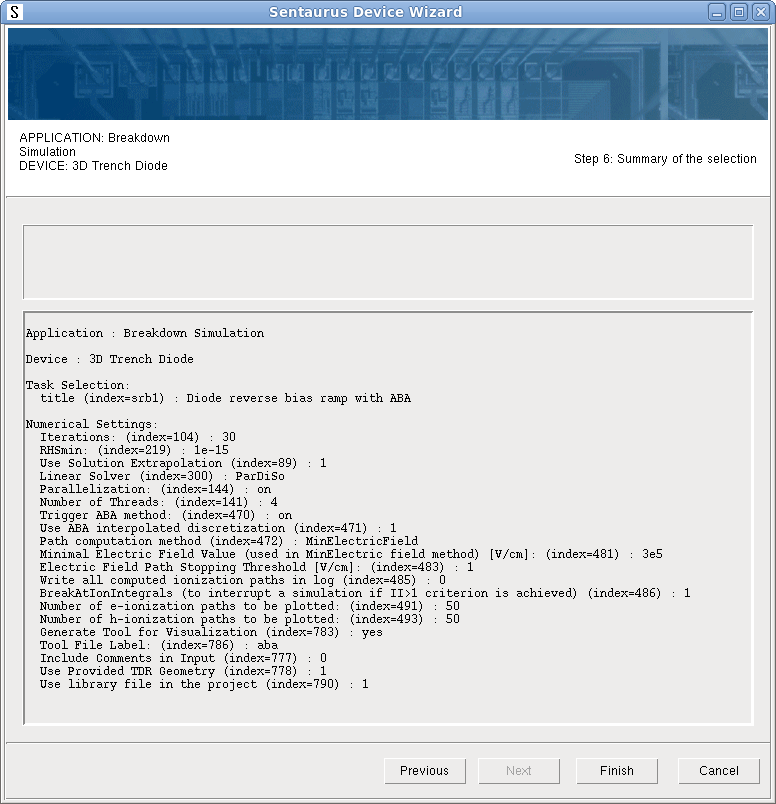
- Click Finish.
The wizard generates the input file for the selected simulation task and opens it in a text editor (see Figure 1). Your default text editor in Sentaurus Workbench is used (jEdit is shown as an example). If a file with a given name already exists, then you will be prompted to confirm whether you want to overwrite it before creating a new one.
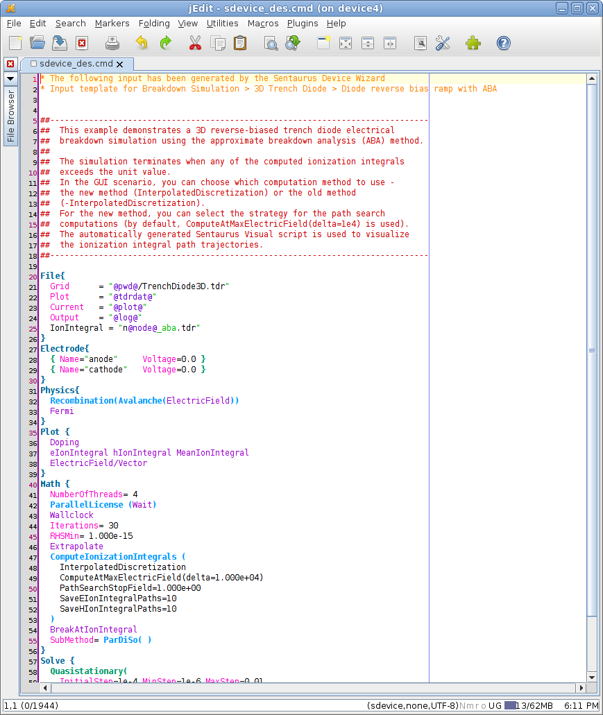
Figure 1. Sentaurus Device command file as generated by Sentaurus Device Wizard. (Click image for full-size view.)
In addition to Sentaurus Device input generation, the Sentaurus Device Wizard creates the subsequent Sentaurus Visual tool instance with a given name and copies its predefined input to the project directory (see Figure 2). To be able to run a device simulation, all relevant files (meshed device structure, parameter file, and so on) are also generated inside the project.
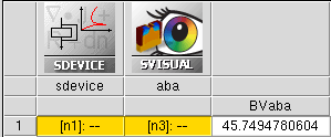
Figure 2. Executed project, generated by using Sentaurus Device Wizard.
Finally, after executing the Sentaurus Device node, you can check the results in Sentaurus Visual (see Figure 3).
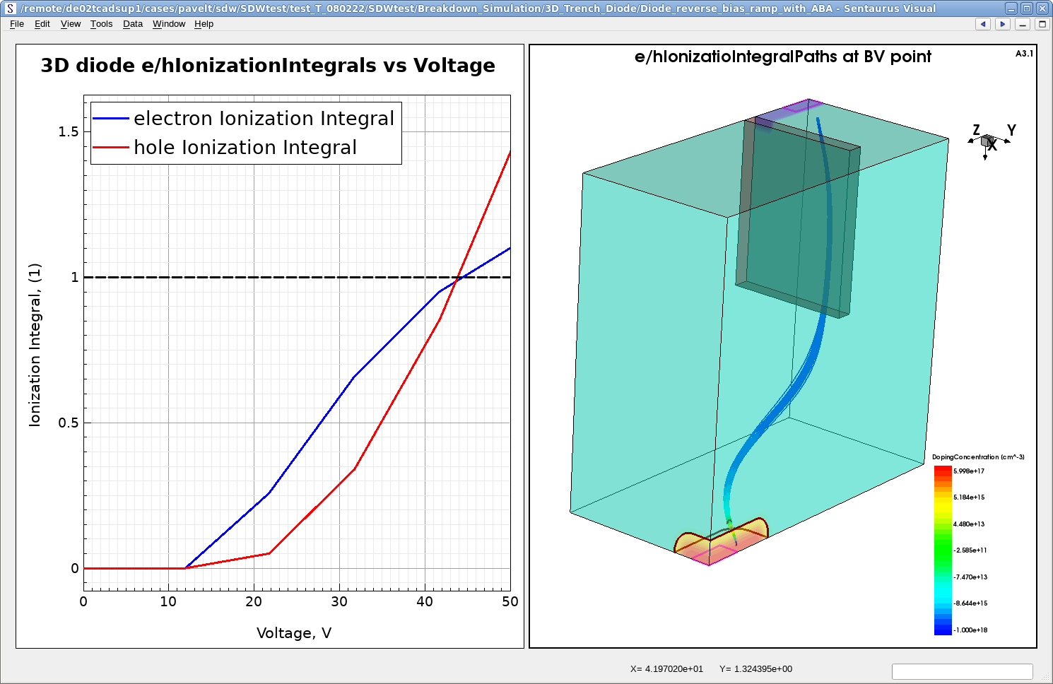
Figure 3. Results of 3D diode simulation with ABA method. (Click image for full-size view.)
Now, you can replace the given device structure with your own device in the project and repeat the device simulation. Before you run it, ensure that all the given electrode names and bias conditions are appropriate for your device.
11.3 Supported Application Examples
Sentaurus Device Wizard supports the following application examples:
- Basic Devices
- Two-Terminal Devices (PDF File)
- 1D p-i-n diode
- 1D Schottky diode
- Zener diode
- 1D MOS capacitor
- 3D resistor
- Three-Terminal Devices (PDF File)
- n-p-n bipolar transistor
- p-n-p bipolar transistor
- Four-Terminal Devices (PDF File)
- Bulk nMOS
- Bulk pMOS
- Two-Terminal Devices (PDF File)
- Power Devices
- Field Termination (PDF File)
- 2D superjunction
- p-i-n junction with multiple guard rings
- Bevel edge termination
- 3D edge-termination
- IGBTs (PDF File)
- Trench Gate n-IGBT
- Power MOSFETs (PDF File)
- 2D laterally diffused NMOSFET
- Thyristors (
PDF File)
- Cylindrically symmetric gate-controlled thyristor
- 2D MOS-controlled thyristor
- Field Termination (PDF File)
- Memory & Logic Devices
- Ferroelectrics (PDF File)
- Ferroelectric capacitor
- Ferroelectric capacitor with nonuniform heat
- Antiferroelectric capacitor
- 1T FeRAM
- Negative capacitance FET
- Multidomain ferroelectric capacitor
- Nonvolatile Memory (PDF File)
- 2D 65 nm flash cell
- 3-bit BiCS NAND flash
- Phase Change Memory (PDF File)
- GeSbTe PCM cell
- Spintronics (PDF File)
- MTJ interlayer exchange coupling
- Ferroelectrics (PDF File)
- Heterojunction Devices
- Wide-Bandgap Devices
- Advanced Devices
- Advanced MOSFETs (PDF File)
- 30 nm FDSOI NMOSFET
- 16 nm silicon NFinFET
- Advanced MOSFETs (PDF File)
- Sensors
- Galvanic (PDF File)
- 2D Hall sensor
- 3D Hall sensor
- Galvanic (PDF File)
- Thin-Film Transistors (PDF File)
- Amorphous Silicon TFT
- 2D self-aligned back gate TFT
- Polysilicon TFT
- 2D multiple grain n-type TFT
- Amorphous Silicon TFT
- Organic Semiconductors
- OTFT (PDF File)
- 2D polythiophene OTFT
- OTFT (PDF File)
- Passive Photonics
- Circuit & Compact Models
- ESD and current protection
- Thermoelectric Devices (PDF File)
- Thermoelectric Power Generators
- Thermoelectric Coolers
- Special Technique Demonstrators
- Breakdown Simulation (PDF File)
- Cyclic Analysis (PDF File)
- Degradation (PDF File)
- LDMOS degradation with R-D model
- PMOS degradation with NBTI model
- NMOS degradation with HCS model
- PMOS degradation with HCS model
- PMOS degradation with hydrogen diffusion model
- Low-Temperature Simulation (PDF File)
- Noise Simulation (PDF File)
- Radiation (PDF File)
- SOIFET gamma dose irradiation
- SOIFET X-ray dose irradiation
- Heavy ion impact on 3D 6T SRAM Cell
- LDMOS heavy ion strike
- NMOSFET alpha particle strike
- Material irradiation with Crystal Ball model (PDF File)
- Si, SiC, GaN, Ge, and GaAs alpha particle irradiation with CB model
- Si, SiC, GaN, Ge, and GaAs proton irradiation with CB model
- Transport in Metals (PDF File)
- Seebeck effect
- Peltier effect
- Variability (PDF File)
- 3D MOSFET random dopant fluctuation with statistical method
- 3D MOSFET random dopant fluctuation with impedance field method
- 3D MOSFET random geometry fluctuation with impedance field method
- Interface trap randomization
- Single trap randomization
- 3D MOSFET metal gate WF randomization
- 2D MOSFET oxide thickness variation with deterministic method
- Sentaurus Device Advanced Use (PDF File)
main menu | module menu | << previous section | next section >>
Copyright © 2024 Synopsys, Inc. All rights reserved.